Printed chemical mechanical polishing pad

Active Publication Date: 2016-04-21
APPLIED MATERIALS INC
View PDF8 Cites 31 Cited by
  • Summary
  • Abstract
  • Description
  • Claims
  • Application Information

AI Technical Summary

Problems solved by technology

Reliably producing nanometer and smaller features is one of the key technology challenges for next generation very large scale integration (VLSI) and ultra large-scale integration (ULSI) of semiconductor devices.
However, as the limits of circuit technology are p

Method used


Image

  • Printed chemical mechanical polishing pad
  • Printed chemical mechanical polishing pad
  • Printed chemical mechanical polishing pad

Examples


Embodiment Construction

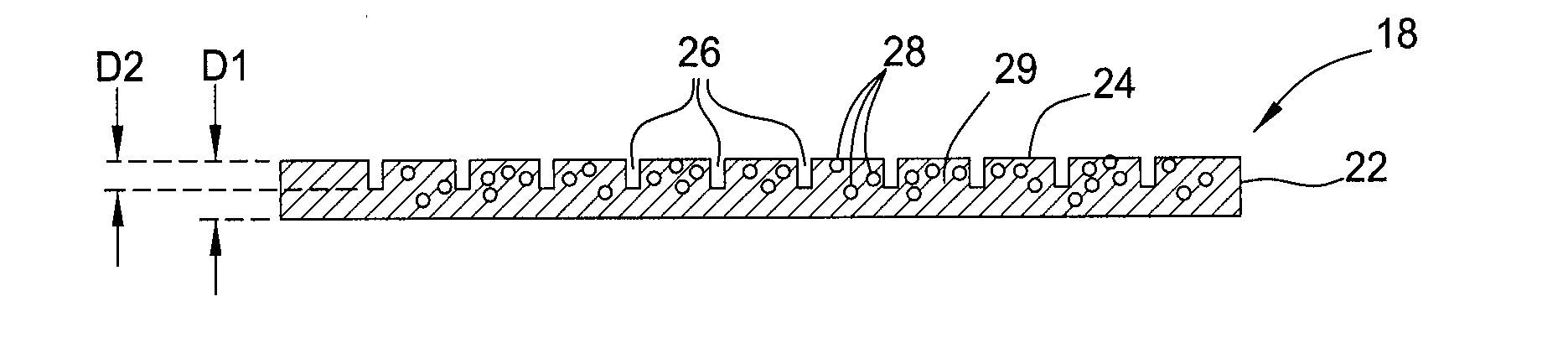
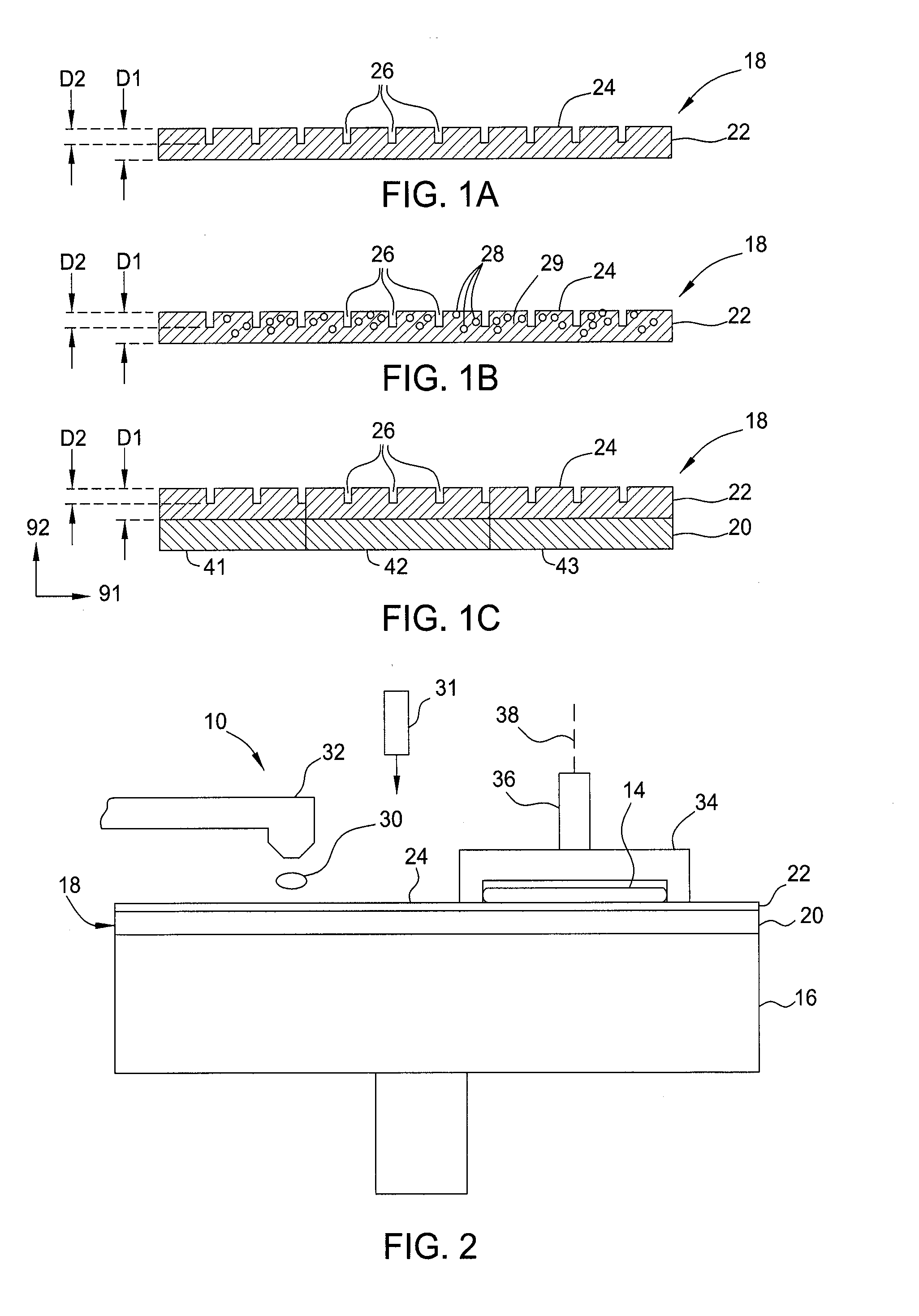
[0019]In order to provide polishing uniformity, a polishing pad needs to form a uniform contact with the substrate being polished, such that uniform pressure can be applied across the substrate surface. A variation in thickness of the pads can create non-uniform pressure across the substrate surface. Even small variations in thickness lead to variations in the applied pressure, and hence non-uniform removal as well as higher defects such as micro-scratches on the substrate surface. This effect is more acute for hard polishing pads, and is also more acute at low pressure polish processes. Although a soft polishing pad can accommodate larger thickness variations, the process of forming grooving in the pad is more likely to generate non-uniformity in soft polishing pads.

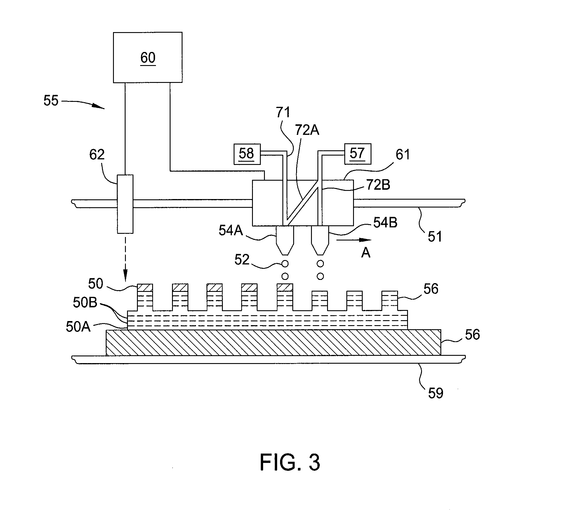
[0020]A technique for manufacturing polishing pads that can provide improved thickness uniformity is 3D printing. In a 3D printing process, a thin layer of pad precursor, e.g., a liquid, is progressively deposited and f...


PUM


Abstract

A method of fabricating a polishing layer of a polishing pad includes successively depositing a plurality of layers with a 3D printer, each layer of the plurality of polishing layers deposited by ejecting a base material from a first nozzle and an additive material from a second nozzle and solidifying the base and additive material to form a solidified pad material.

Description

CROSS-REFERENCE TO RELATED APPLICATIONS[0001]This application claims benefit of U.S. Provisional Application Ser. No. 62 / 065,190, filed Oct. 17, 2014 (Attorney Docket No. APPM / 22348USL), and U.S. Provisional Application Ser. No. 62 / 066,291, filed Oct. 20, 2014 (Attorney Docket No. APPM / 22348USL02), both of which are incorporated by reference in their entirety.BACKGROUND[0002]1. Field[0003]This present invention relates to polishing pads used in chemical mechanical polishing.[0004]2. Description of the Related Art[0005]Reliably producing nanometer and smaller features is one of the key technology challenges for next generation very large scale integration (VLSI) and ultra large-scale integration (ULSI) of semiconductor devices. However, as the limits of circuit technology are pushed, the shrinking dimensions of VLSI and ULSI interconnect technology have placed additional demands on processing capabilities. Reliable formation of gate structures on the substrate is important to VLSI an...

Claims


Application Information

Patent Timeline
IPC IPC(8): B24B37/24B24B37/26B24D18/00B24B37/22
CPCB24B37/24B24B37/22B33Y80/00B24D18/0045B33Y10/00B24B37/26B24B37/245
Inventor ORILALL, MAHENDRA CHRISTOPHERMICHAELSON, TIMOTHYKRISHNAN, KASIRAMANBAJAJ, RAJEEVPATIBANDLA, NAG B.REDFIELD, DANIELREDEKER, FRED C.MENK, GREGORY E.
Owner APPLIED MATERIALS INC
Why Eureka
Try Eureka