Programming method for NAND-type flash memory
a programming method and flash memory technology, applied in static storage, digital storage, instruments, etc., can solve the problems of inability to ensure reliability, limited number of rewriting data, and degradation of the film quality of the oxide film under the floating gate, so as to reduce the shorten the period from the erase operation to the programming operation, and increase the maximum number of data rewritings
- Summary
- Abstract
- Description
- Claims
- Application Information
AI Technical Summary
Benefits of technology
Problems solved by technology
Method used
Image
Examples
embodiment 1
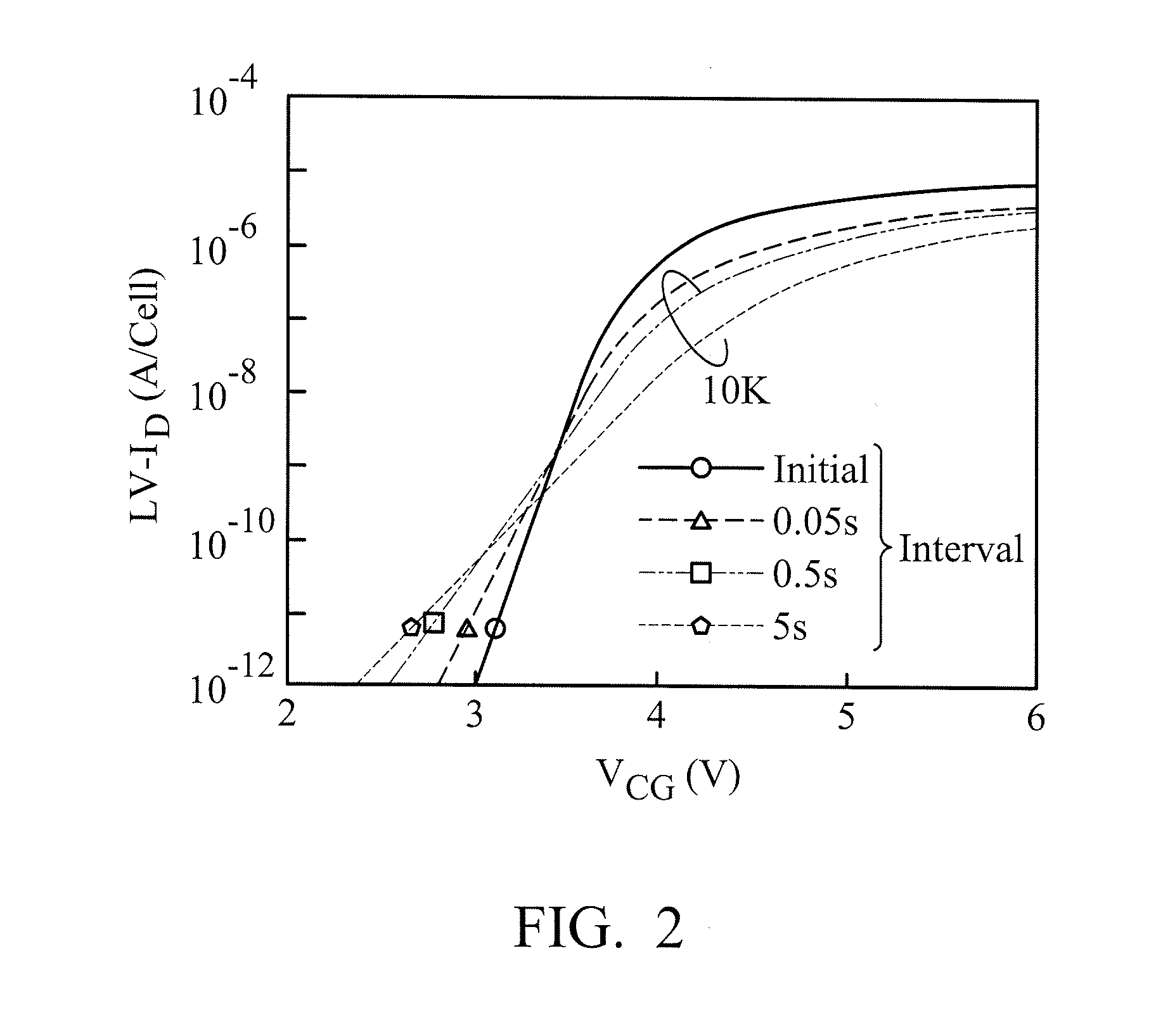
[0029]Next, a programming method in accordance with Embodiment 1 of the invention is illustrated. In a preferred aspect of the embodiment, in order to improve the rewriting ability (endurance ability) of the memory cell, the period from the erase operation to the programming (write-in) operation on the same block is shortened as much as possible. In a more preferred aspect of the embodiment, the period from the programming (write-in) operation to the erase operation on the same block is extended as much as possible, which helps the recovery of the tunnel oxide film of the memory cell and improves the rewriting ability.
[0030]FIG. 5 is a flowchart for illustrating a programming method of Embodiment 1. First, the controller 150 determines whether the flash memory has to enter to a block programming mode according to a command received from an external host device via the input / output buffer 120. “Block programming” in the embodiment means a mode to page program data into a plurality of...
embodiment 2
[0045], the erasing of the selected block is performed during the period where the data to be programmed is loaded into the cache memory 300 connected to the exterior of the flash memory 100. The data loaded into the cache memory 300 can immediately be programmed to the erased block. Thereby, degradation due to data rewriting of the memory cell can be reduced.
[0046]Embodiment 2 shows an example of the cache memory 300 being connected to the exterior of the flash memory 100 and the flash memory 100 having a built-in cache memory 140. However, in order to raise the speed of the block programming (namely, in order to shorten the loading time of data from the cache memory 300 to the page buffer / sense circuit 170), it is also appropriate that the data is moved from the cache memory 300 into the cache memory 140 or the page buffer / sense circuit 170 before the cache programming is started. Furthermore, in cases where the cache memory 300 is connected to the exterior of the cache memory 100...
PUM
 Abstract
Description
Claims
Application Information


