Method And System For Germanium-On-Silicon Photodetectors Without Germanium Layer Contacts

Active Publication Date: 2016-06-02
CISCO TECH INC
View PDF5 Cites 26 Cited by
  • Summary
  • Abstract
  • Description
  • Claims
  • Application Information

AI Technical Summary

Benefits of technology

[0004]Further limitations and disadvantages of conventional and traditional approaches will become apparent to one of skill in the art, through

Problems solved by technology

They can be mitigated to some extent with equalization, coding, and shielding, but these techniques require considerable

Method used


Image

  • Method And System For Germanium-On-Silicon Photodetectors Without Germanium Layer Contacts
  • Method And System For Germanium-On-Silicon Photodetectors Without Germanium Layer Contacts
  • Method And System For Germanium-On-Silicon Photodetectors Without Germanium Layer Contacts

Examples


Embodiment Construction

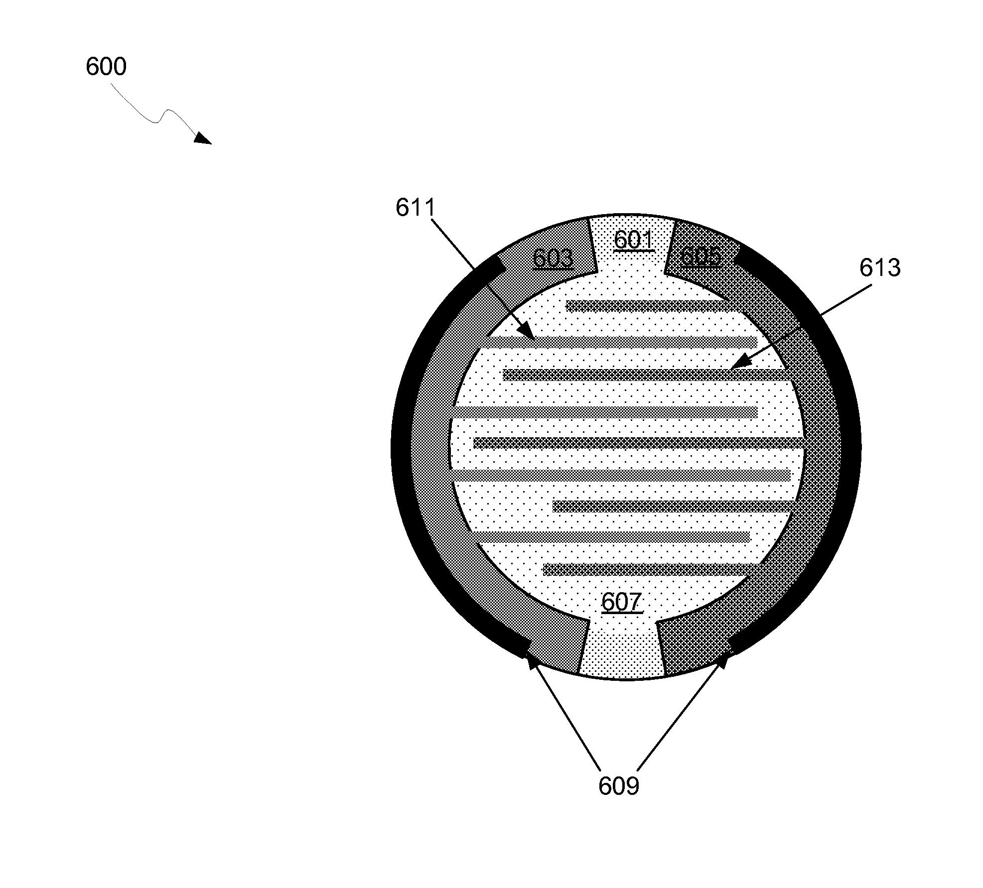
[0020]Certain aspects of the disclosure may be found in a method and system for germanium-on-silicon photodetectors without germanium layer contacts. Exemplary aspects of the disclosure may comprise, in a semiconductor die having a photodetector comprising an n-type silicon layer, a germanium layer, a p-type silicon layer, and a metal contact on each of the n-type silicon layer and the p-type silicon layer: receiving an optical signal, absorbing the optical signal in the germanium layer, generating an electrical signal from the absorbed optical signal, and communicating the electrical signal out of the photodetector via the n-type silicon layer and the p-type silicon layer. The photodetector may comprise a horizontal junction double heterostructure where the germanium layer is above the n-type silicon layer and the p-type silicon layer. An intrinsically-doped silicon layer may be below the germanium layer between the n-type silicon layer and the p-type silicon layer. A portion of th...


PUM


Abstract

Methods and systems for germanium-on-silicon photodetectors without germanium layer contacts are disclosed and may include, in a semiconductor die having a photodetector, where the photodetector includes an n-type silicon layer, a germanium layer, a p-type silicon layer, and a metal contact on each of the n-type silicon layer and the p-type silicon layer: receiving an optical signal, absorbing the optical signal in the germanium layer, generating an electrical signal from the absorbed optical signal, and communicating the electrical signal out of the photodetector via the n-type silicon layer and the p-type silicon layer. The photodetector may include a horizontal or vertical junction double heterostructure where the germanium layer is above the n-type and p-type silicon layers. An intrinsically-doped silicon layer may be below the germanium layer between the n-type silicon layer and the p-type silicon layer. A top portion of the germanium layer may be p-doped.

Description

CROSS-REFERENCE TO RELATED APPLICATIONS / INCORPORATION BY REFERENCE[0001]This application claims priority to and the benefit of U.S. Provisional Application 62 / 086,137 filed on Dec. 1, 2014, which is hereby incorporated herein by reference in its entirety.FIELD[0002]Certain embodiments of the disclosure relate to semiconductor photonics. More specifically, certain embodiments of the disclosure relate to a method and system for germanium-on-silicon photodetectors without germanium layer contacts.BACKGROUND[0003]As data networks scale to meet ever-increasing bandwidth requirements, the shortcomings of copper data channels are becoming apparent. Signal attenuation and crosstalk due to radiated electromagnetic energy are the main impediments encountered by designers of such systems. They can be mitigated to some extent with equalization, coding, and shielding, but these techniques require considerable power, complexity, and cable bulk penalties while offering only modest improvements in ...

Claims


Application Information

Patent Timeline
IPC IPC(8): H01L31/11H01L31/0352H01L31/028
CPCH01L31/11H01L31/03529H01L31/028H01L31/08H01L31/1812G02B6/4292H01L31/022408H01L31/103H01L31/105H01L31/109H01L31/022416
Inventor HON, KAM-YANMASINI, GIANLORENZOSAHNI, SUBAL
Owner CISCO TECH INC
Why Eureka
Try Eureka