Micro LED with dielectric side mirror

a dielectric side mirror and micro led technology, applied in the direction of basic electric elements, electrical equipment, semiconductor devices, etc., can solve problems such as deterioration of contrast ratio

Inactive Publication Date: 2016-06-23
APPLE INC
View PDF7 Cites 50 Cited by
  • Summary
  • Abstract
  • Description
  • Claims
  • Application Information

AI Technical Summary

Benefits of technology

[0009]In an embodiment, an electronic device includes a display substrate and a plurality of vertical LEDs bonded to a corresponding plurality of driver contacts in a display region of the display substrate. In an embodiment, a transparent protective cover plate is secured over the display region of the display substrate, and a polarizer film is not located between the transparent protective cover plate and the display substrate. The transparent protective cover plate is exposed to ambient atmosphere.
[0010]As described above, the opening formed in the dielectric mirror for each vertical LED may include tapered sidewalls. The

Problems solved by technology

When an OLED display is observed in a bright environment, reflection from

Method used


Image

  • Micro LED with dielectric side mirror
  • Micro LED with dielectric side mirror
  • Micro LED with dielectric side mirror

Examples


Embodiment Construction

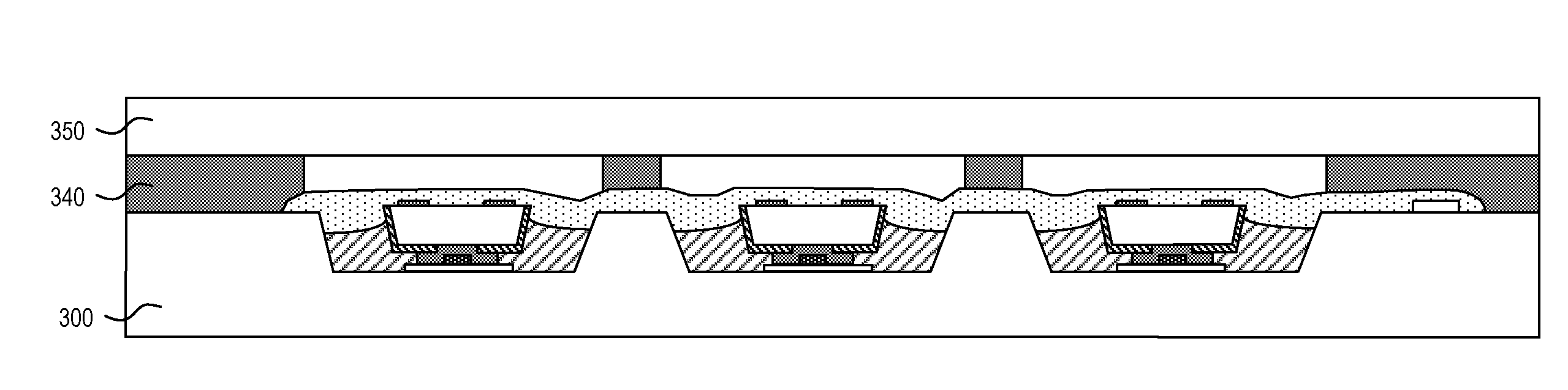
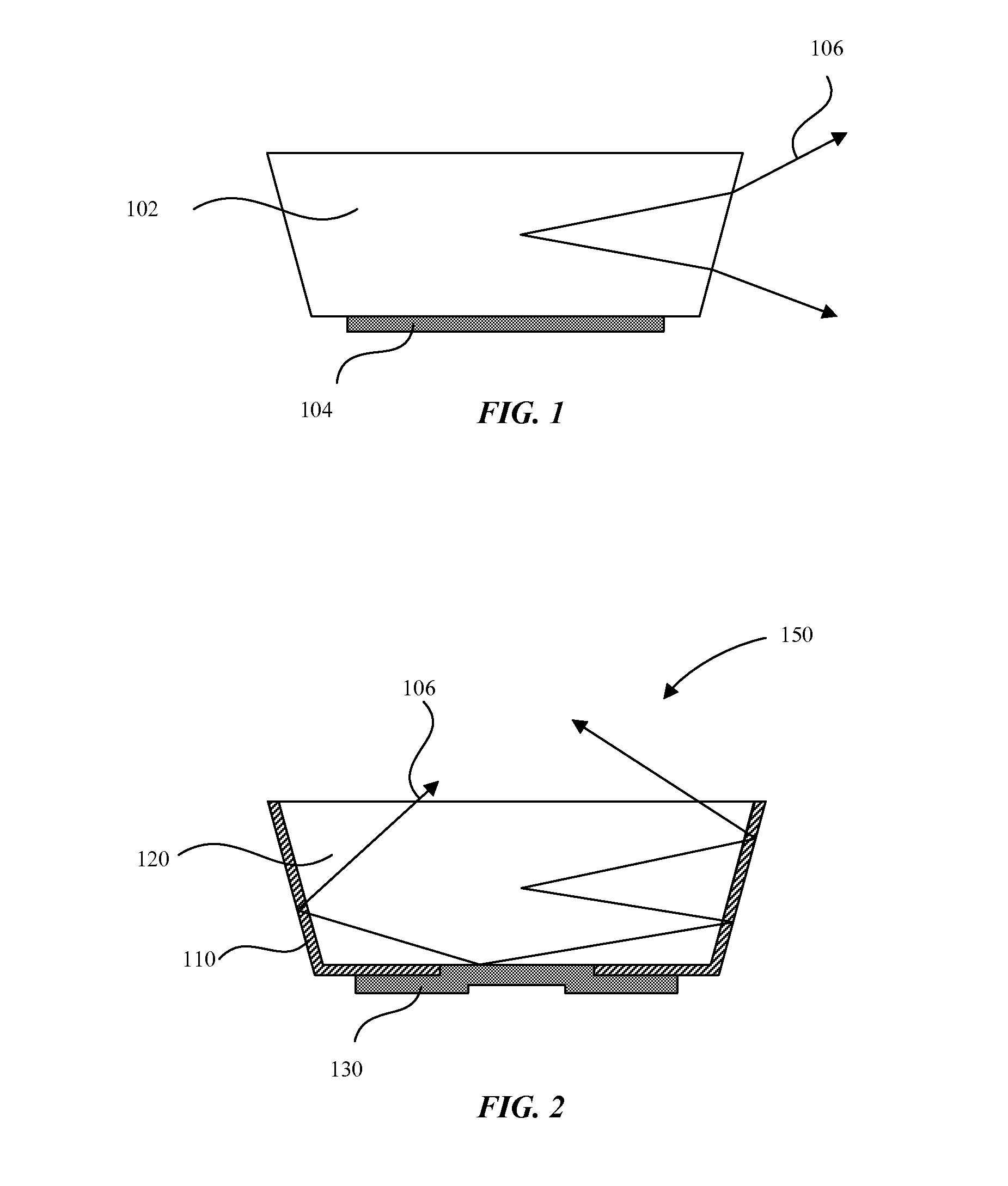
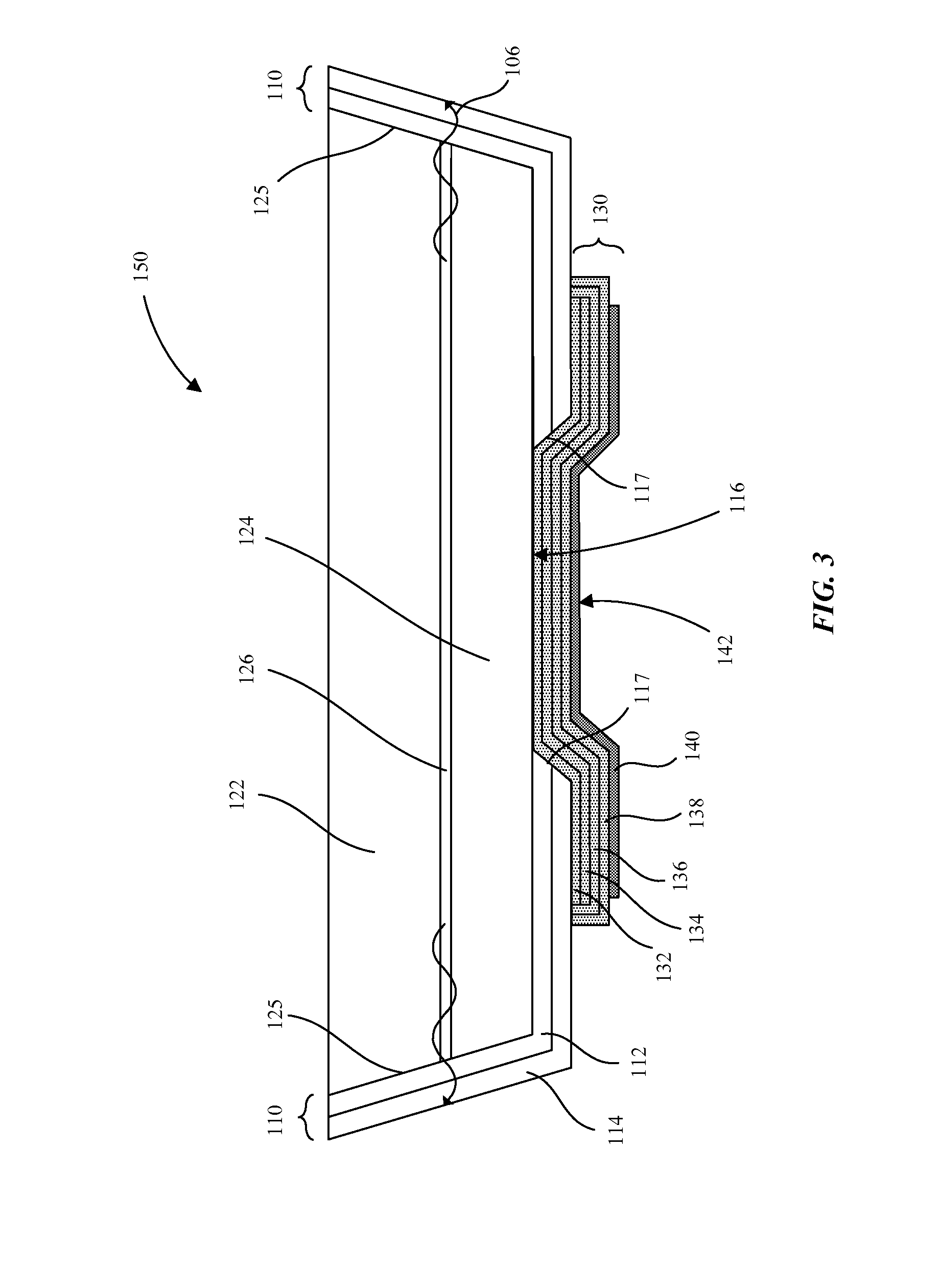
[0030]Embodiments describe LEDs including integrated dielectric mirrors, and LED integration schemes for electronic devices. In various embodiments, description is made with reference to figures. However, certain embodiments may be practiced without one or more of these specific details, or in combination with other known methods and configurations. In the following description, numerous specific details are set forth, such as specific configurations, dimensions and processes, etc., in order to provide a thorough understanding of the embodiments. In other instances, well-known semiconductor processes and manufacturing techniques have not been described in particular detail in order to not unnecessarily obscure the embodiments. Reference throughout this specification to “one embodiment” means that a particular feature, structure, configuration, or characteristic described in connection with the embodiment is included in at least one embodiment. Thus, the appearances of the phrase “in...


PUM


Abstract

LEDs and an electronic device are disclosed. In an embodiment an LED includes a p-n diode and a dielectric mirror spanning along a lateral sidewall of the p-n diode and directly underneath the p-n diode. An opening is formed in the dielectric mirror directly underneath the p-n diode, and a bottom conductive contact is on the dielectric mirror directly underneath the p-n diode and within the opening in the dielectric mirror.

Description

RELATED APPLICATIONS[0001]This application claims the benefit of priority from U.S. Provisional Application No. 62 / 093,078, filed on Dec. 17, 2014, which is herein incorporated by reference.BACKGROUND[0002]1. Field[0003]Embodiments relate to light emitting diodes. More particularly embodiments relate to a light emitting diode with a dielectric mirror.[0004]2. Background Information[0005]Light emitting diodes (LEDs) are increasingly being considered as a replacement technology for existing light sources. For example, LEDs are found in signage, traffic signals, automotive tail lights, mobile electronics displays, and televisions. Various benefits of LEDs compared to traditional lighting sources may include increased efficiency, longer lifespan, variable emission spectra, and the ability to be integrated with various form factors.[0006]One type of LED is an organic light emitting diode (OLED) in which the emissive layer of the diode is formed of an organic compound. One advantage of OL...

Claims


Application Information

Patent Timeline
IPC IPC(8): H01L33/38H01L33/48H01L33/60H01L25/075H01L33/06H01L33/62
CPCH01L33/38H01L33/06H01L33/483H01L33/60H01L25/0753H01L33/62H01L24/83H01L24/95H01L33/0093H01L33/20H01L33/46H01L2924/0002H01L2924/00
Inventor CHANG, KEVIN K. C.HU, HSIN-HUACHAN, CLAYTON KA TSUNHUANG, CHIEN-HSING
Owner APPLE INC
Why Eureka
Try Eureka