
Tunable-frequency pulse forming networks for high power microwave applications

Inactive Publication Date: 2016-06-30
BAE SYST INFORMATION & ELECTRONICS SYST INTERGRATION INC
View PDF0 Cites 3 Cited by
  • Summary
  • Abstract
  • Description
  • Claims
  • Application Information

AI Technical Summary

Benefits of technology

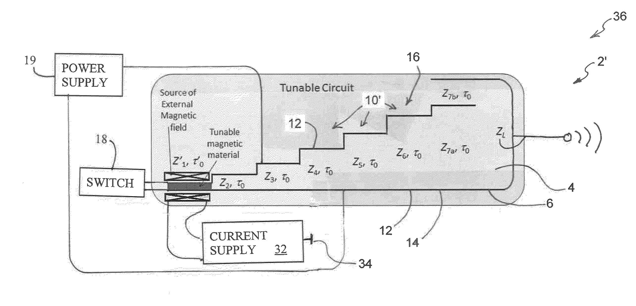
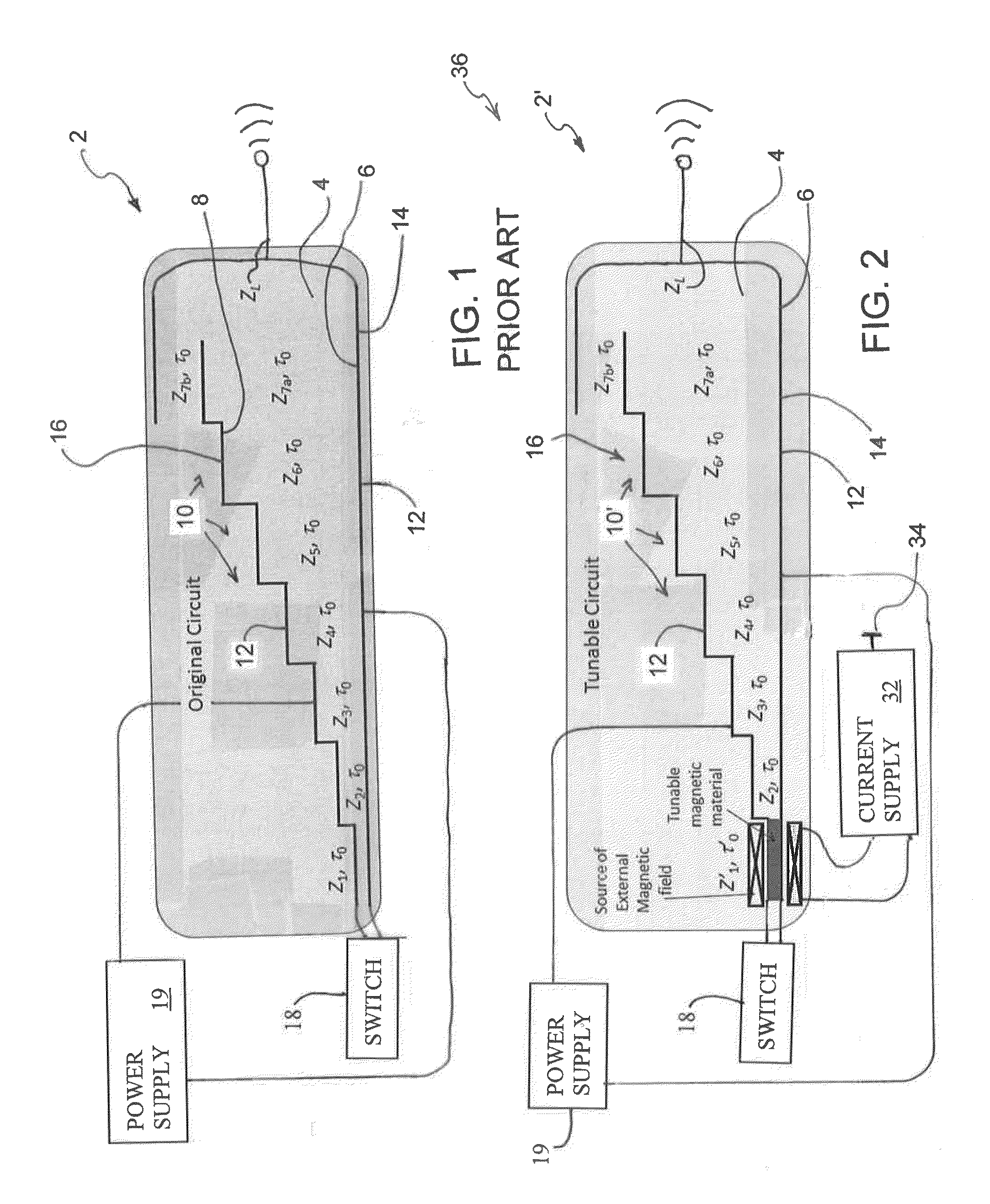
The invention is a tunable-frequency pulse forming network that can change the waveform and spectral content of a high-power microwave signal in a surrounding environment. By replacing the dielectric filling of the transmission line segments with nonlinear material, the effective electrical length is changed to control the pulse duration and spectral content. The circuit has a compact design with a small footprint and is suitable for use in high-speed frequency agility applications. The pulse forming network circuit includes a dielectric material, a ground section, a stepped charged section, a power supply, a switch, and an antenna. The technical effect of the invention is that a tunable-frequency pulse forming network can be easily designed to change the waveform and spectral content of a high-power microwave signal in a surrounding environment, which is useful in various applications such as radar systems or microwave communication systems. This technology allows for high-speed frequency agility and increases the flexibility of the circuit design.

Problems solved by technology

However, potential customers indicate a lot of interest in frequency agile HPM sources and in sources capable of generating arbitrary waveforms since different targets are vulnerable to different frequencies and different waveforms.

Method used


Image

  • Tunable-frequency pulse forming networks for high power microwave applications
  • Tunable-frequency pulse forming networks for high power microwave applications
  • Tunable-frequency pulse forming networks for high power microwave applications

Examples


Embodiment Construction

[0032]The present invention will be understood by reference to the following detailed description, which should be read in conjunction with the appended drawings. It is to be appreciated that the following detailed description of various embodiments is by way of example only and is not meant to limit, in any way, the scope of the present invention.

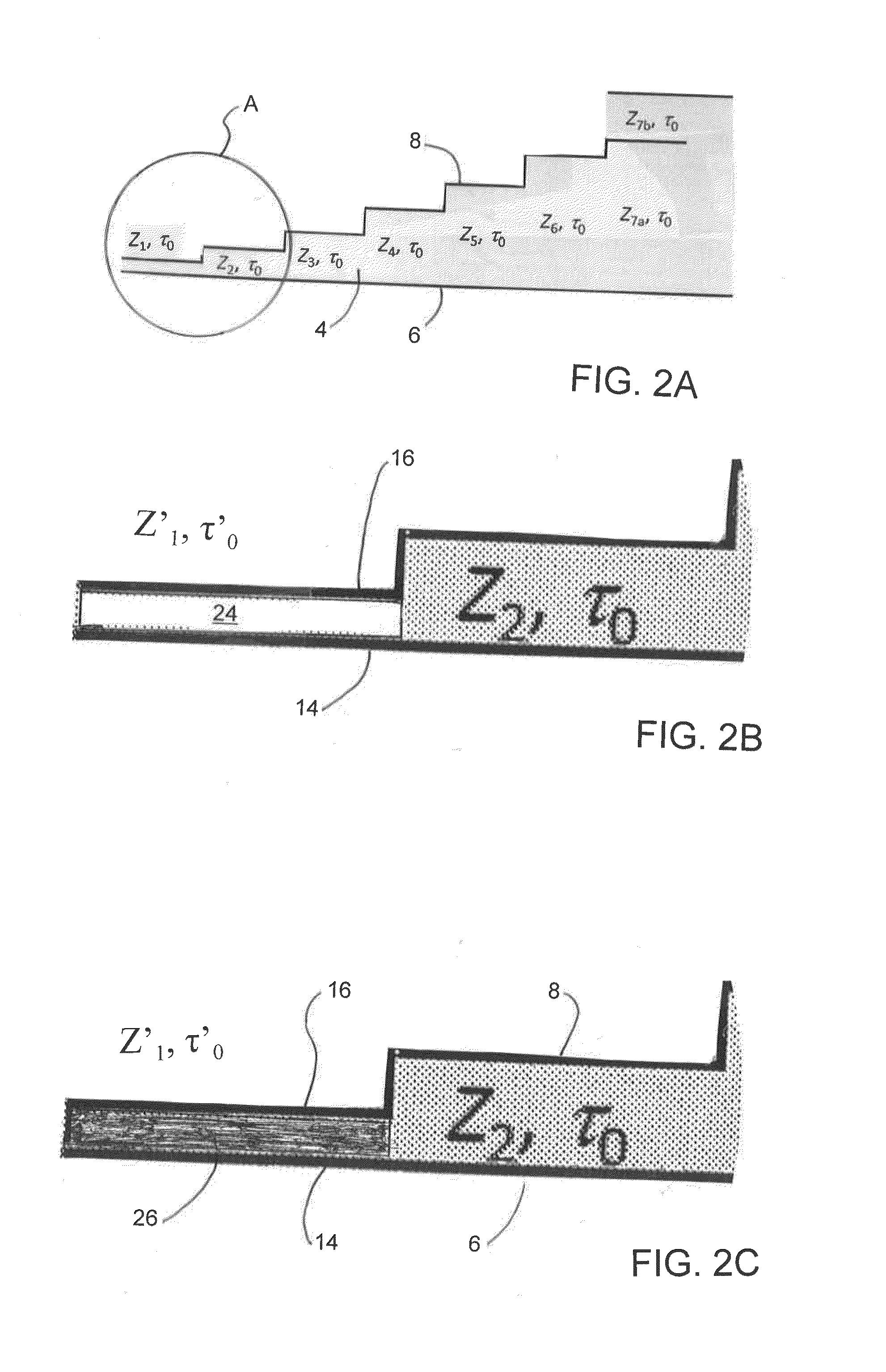
[0033]FIG. 2 is a diagrammatic Fig. showing, as an example, a single-cycle PFN circuit 2′ according to the present invention. In order to form such single-cycle PFN circuit 2′, the dielectric material 4 is first cut or otherwise shaped into the basic shape of the single-cycle PFN circuit 2′ as generally shown in FIG. 2A. Next, the dielectric material 4, located between the first step or stage Z1 of the charged section 16 and the ground section 14 of the circuit 2′, is substantially cut out and / or removed, as generally shown in FIG. 2B. As shown in this Figure, a substantial portion of the entire dielectric material 4, located between the f...


PUM


Abstract

A tunable frequency transmission line pulse forming network circuit for forming a waveform having a spectral content. The pulse forming network circuit comprises a dielectric material; a ground section; a stepped shaped charged section, with the charged section having a plurality of stages including a first stage; a power supply coupled to the pulse forming network circuit for charging the pulse forming network circuit; a switch coupled to the pulse forming network circuit for periodically discharging the pulse forming network circuit; and an antenna coupled to the pulse forming network circuit for propagating a high-power microwave signal from the pulse forming network circuit into the environment. At least the first stage of pulse forming network circuit has one of a tunable magnetic material and a nonlinear magnetic which facilitates adjusting the waveform and the spectral content of the waveform emitted by the pulse forming network circuit into the surrounding environment.

Description

BACKGROUND OF THE INVENTION[0001]1. Field of the Invention[0002]This invention relates to directed energy weapons, and more particularly, to high power microwave weapons.[0003]2. Brief Description of Related Art[0004]Conventional high power microwave (HPM) sources incorporating pulse forming networks (PFNs) based on segments of charged transmission lines (also known as a family of Darlington circuits) have fixed spectral content which is determined by the electrical length. However, potential customers indicate a lot of interest in frequency agile HPM sources and in sources capable of generating arbitrary waveforms since different targets are vulnerable to different frequencies and different waveforms.[0005]As is conventional in the art and used within this patent application, a pulse forming network (PFN) is an electric circuit that accumulates electrical energy over a comparatively long time, then releases this stored energy in the form of a relatively square pulse of a comparativ...

Claims


Application Information

Patent Timeline
IPC IPC(8): G01S7/38
CPCG01S7/38H03K3/53
Inventor KOZYREV, ALEXANDER B.LONDON, SIMON Y.
Owner BAE SYST INFORMATION & ELECTRONICS SYST INTERGRATION INC
Learn More