3D VLSI Interconnection Network with Microfluidic Cooling, Photonics and Parallel Processing Architecture

a technology of photonics and parallel processing, applied in the field of three-dimensional vlsi architecture, can solve the problems of limiting the performance of large machines, bandwidth and latency of switches are often performance bottlenecks, and programmers have no choice but to labor hard

Active Publication Date: 2016-06-30
VISHKIN UZI Y
View PDF8 Cites 6 Cited by
  • Summary
  • Abstract
  • Description
  • Claims
  • Application Information

AI Technical Summary

Benefits of technology

[0024]Another representative embodiment discloses a three-dimensional VLSI integrated circuit apparatus comprising first and second VLSI layers, and optionally third and fourth VLSI layers. A first VLSI layer comprises a plurality of first VLSI sublayers, a first silicon sublayer of the plurality of first VLSI sublayers coupleable to at least one heat sink, and a first active silicon sublayer of the plurality of first VLSI sublayers comprising a first plurality of photonic transceivers. A second VLSI layer is coupled to the first VLSI layer, with the second VLSI layer comprising a plurality of second VLSI sublayers, a second silicon sublayer of the plurality of second VLSI sublayers comprising a first plurality of microfluidic cooling channels, and a second active silicon sublayer of the plurality of second VLSI sublayers comprising an interconnection network. In a representative embodiment, the first VLSI layer further comprises: a first metal sublayer of the plurality of first VLSI sublayers, the first metal sublayer comprising a first plurality of through-silicon vias coupling one or more photonic transceivers of the first plurality of photonic transce

Problems solved by technology

However, the need for communication is broader than that:1. The current capacity of communication switches limit performance of large machines.
Bandwidth and latency of switches are often performance bottlenecks for large parallel computers.
Consequently, commercial parallel systems have been evolving away from a flat memory abstraction, for example without any multi-core (or GPU) machine in the market t

Method used


Image

  • 3D VLSI  Interconnection Network with Microfluidic Cooling, Photonics and Parallel Processing Architecture
  • 3D VLSI  Interconnection Network with Microfluidic Cooling, Photonics and Parallel Processing Architecture
  • 3D VLSI  Interconnection Network with Microfluidic Cooling, Photonics and Parallel Processing Architecture

Examples


Embodiment Construction

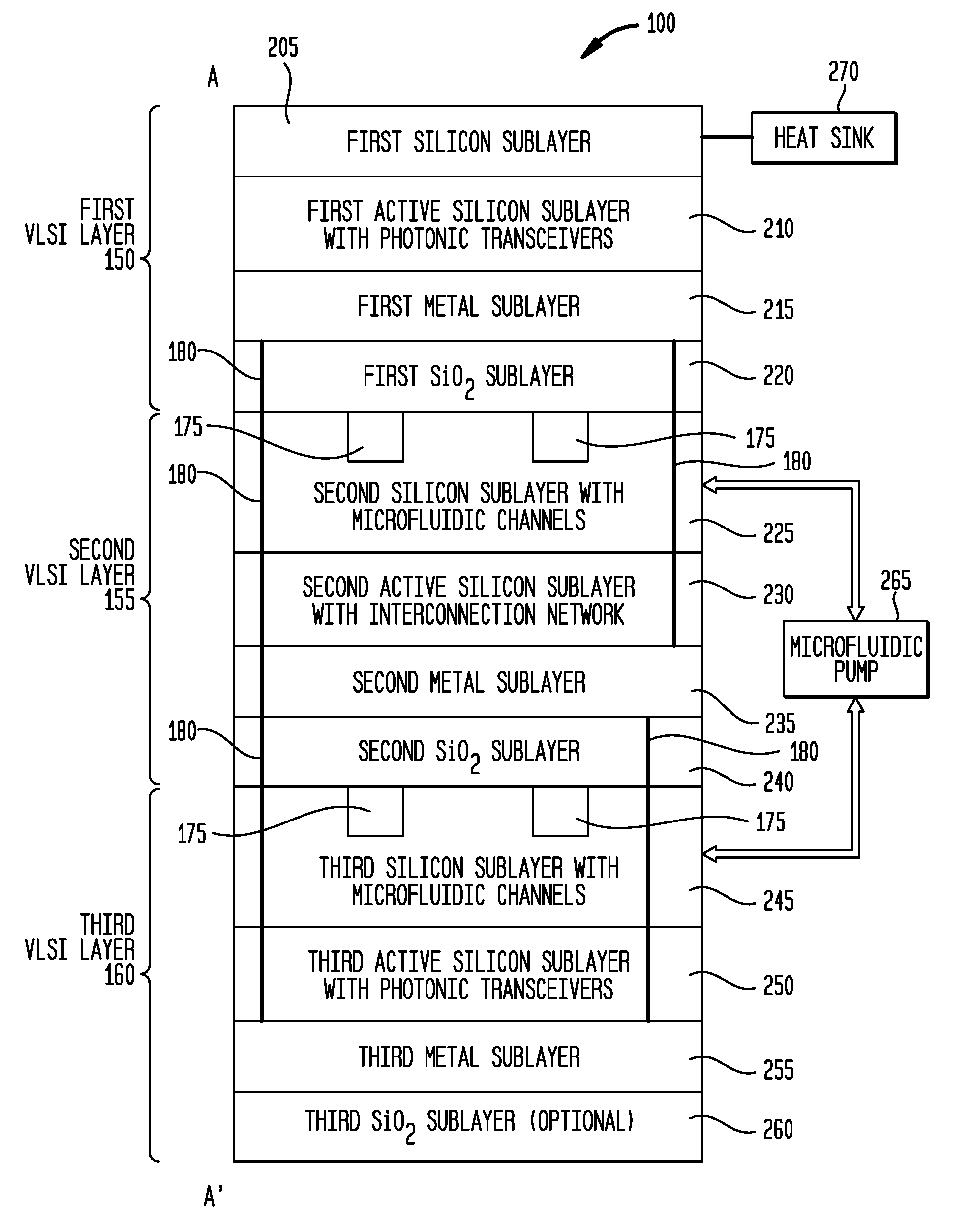
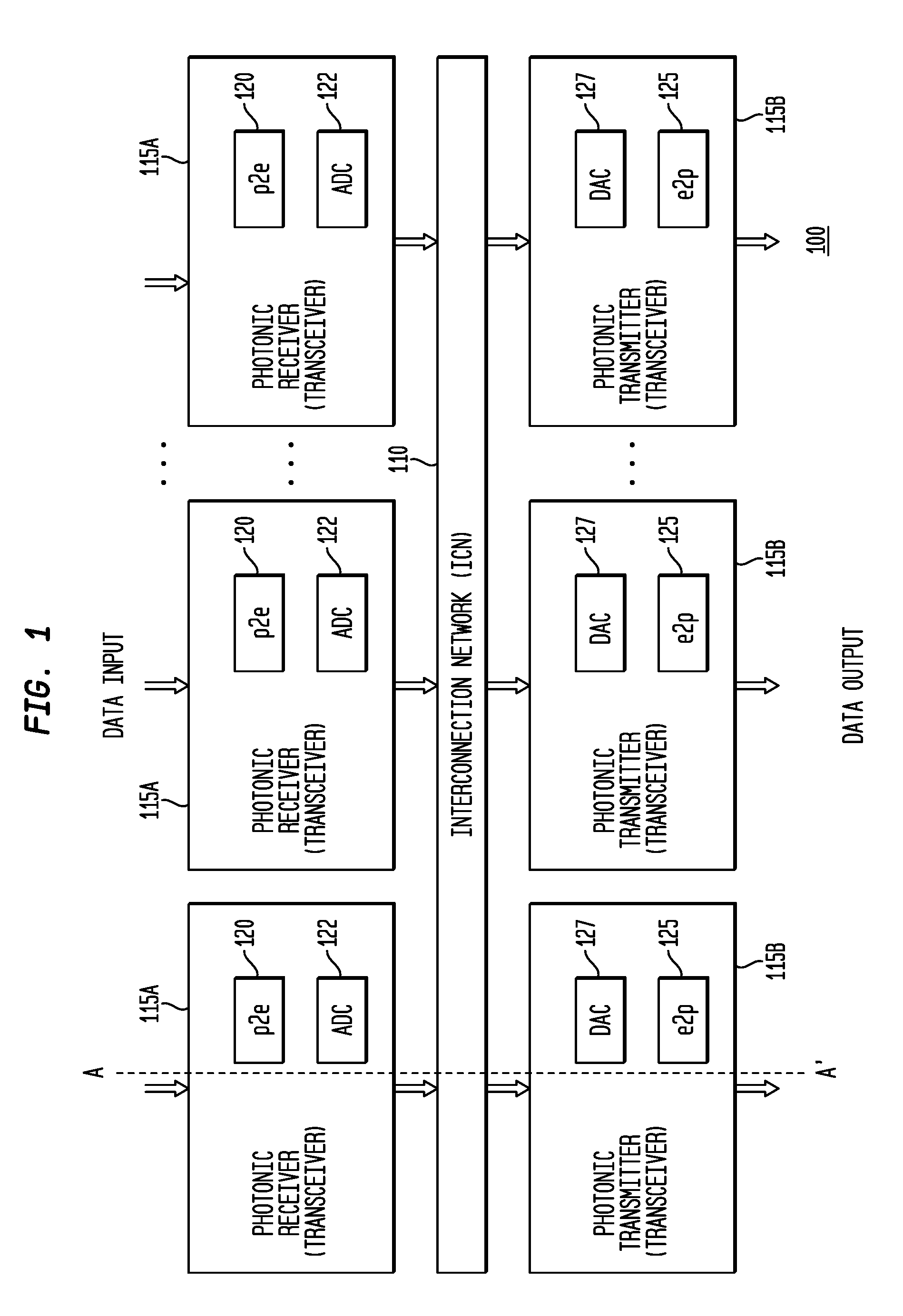
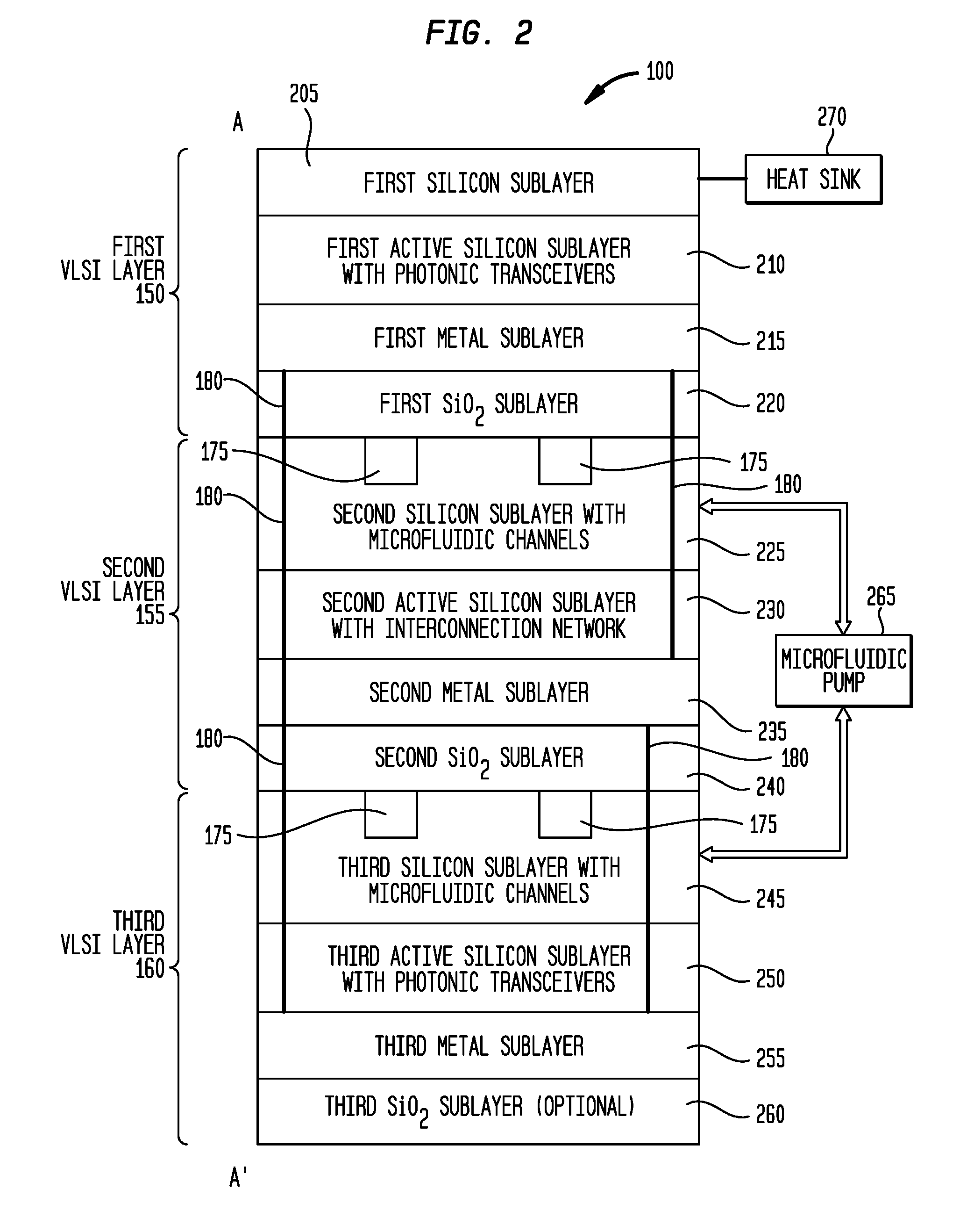
[0040]While the present invention is susceptible of embodiment in many different forms, there are shown in the drawings and will be described herein in detail specific exemplary embodiments thereof, with the understanding that the present disclosure is to be considered as an exemplification of the principles of the invention and is not intended to limit the invention to the specific embodiments illustrated. In this respect, before explaining at least one embodiment consistent with the present invention in detail, it is to be understood that the invention is not limited in its application to the details of construction and to the arrangements of components set forth above and below, illustrated in the drawings, or as described in the examples. Methods and apparatuses consistent with the present invention are capable of other embodiments and of being practiced and carried out in various ways. Also, it is to be understood that the phraseology and terminology employed herein, as well as...


PUM


Abstract

A three-dimensional VLSI integrated circuit apparatus is disclosed having a plurality of VLSI layers. A first VLSI layer includes a first silicon sublayer coupleable to at least one heat sink, and a first active silicon sublayer having a (first) plurality of photonic receivers (or transceivers); and a second VLSI layer including a second silicon sublayer having a first plurality of microfluidic cooling channels, and a second active silicon sublayer of the plurality of second VLSI sublayers having an interconnection network. Additional VLSI layers may also include a third VLSI layer having a third silicon sublayer having a second plurality of microfluidic cooling channels and a third active silicon sublayer having a (second) plurality of photonic transmitters (or transceivers). Additional VLSI layers may also include a third VLSI layer having microfluidic cooling channels and memory circuits, and a fourth VLSI layer having microfluidic cooling channels and parallel processing circuitry.

Description

CROSS-REFERENCE TO A RELATED APPLICATION[0001]This application is a nonprovisional of and claims priority to and the benefit of U.S. Provisional Patent Application No. 62 / 096,539, filed Dec. 24, 2014, inventor Uzi Y. Vishkin, titled “Harness Enabling Technologies for Enhancing Data Movement in Computing Devices and Systems”, the entire contents of which is incorporated herein by reference with the same full force and effect as if set forth in its entirety herein, and with priority claimed for all commonly disclosed subject matter.FIELD OF THE INVENTION[0002]The present invention relates, in general, to interconnection networks for data movement and, more particularly, to a three dimensional VLSI architecture having multiple layers with an interconnection network and a parallel processing circuit architectures with microfluidic cooling and photonic transceivers.BACKGROUND OF THE INVENTION[0003]In serial computing, communication was needed between the processor and memory. Starting ar...

Claims


Application Information

Patent Timeline
IPC IPC(8): G02B6/12G02B6/42
CPCG02B6/12002G02B6/12004G02B2006/12135G02B2006/12123G02B2006/12061G02B6/4268
Inventor VISHKIN, UZI Y.
Owner VISHKIN UZI Y
Why Eureka
Try Eureka