Low voltage nanoscale vacuum electronic devices

a vacuum electronic device, low-voltage technology, applied in the direction of discharge tube/lamp details, basic electric elements, radiation control devices, etc., can solve the problem of careful design of materials and structures

Inactive Publication Date: 2016-07-07
UNIV OF PITTSBURGH OF THE COMMONWEALTH SYST OF HIGHER EDUCATION
View PDF3 Cites 5 Cited by
  • Summary
  • Abstract
  • Description
  • Claims
  • Application Information

AI Technical Summary

Benefits of technology

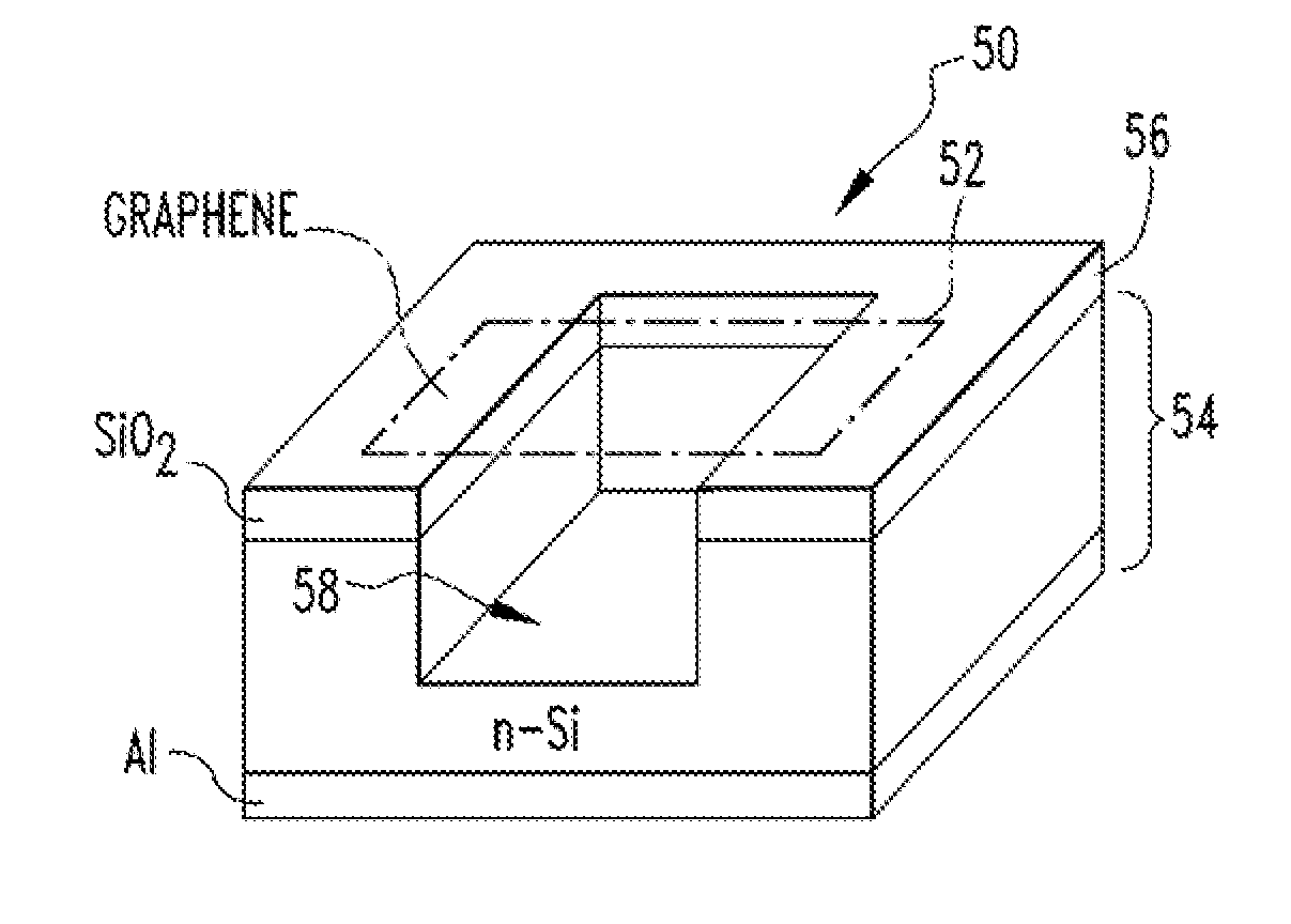
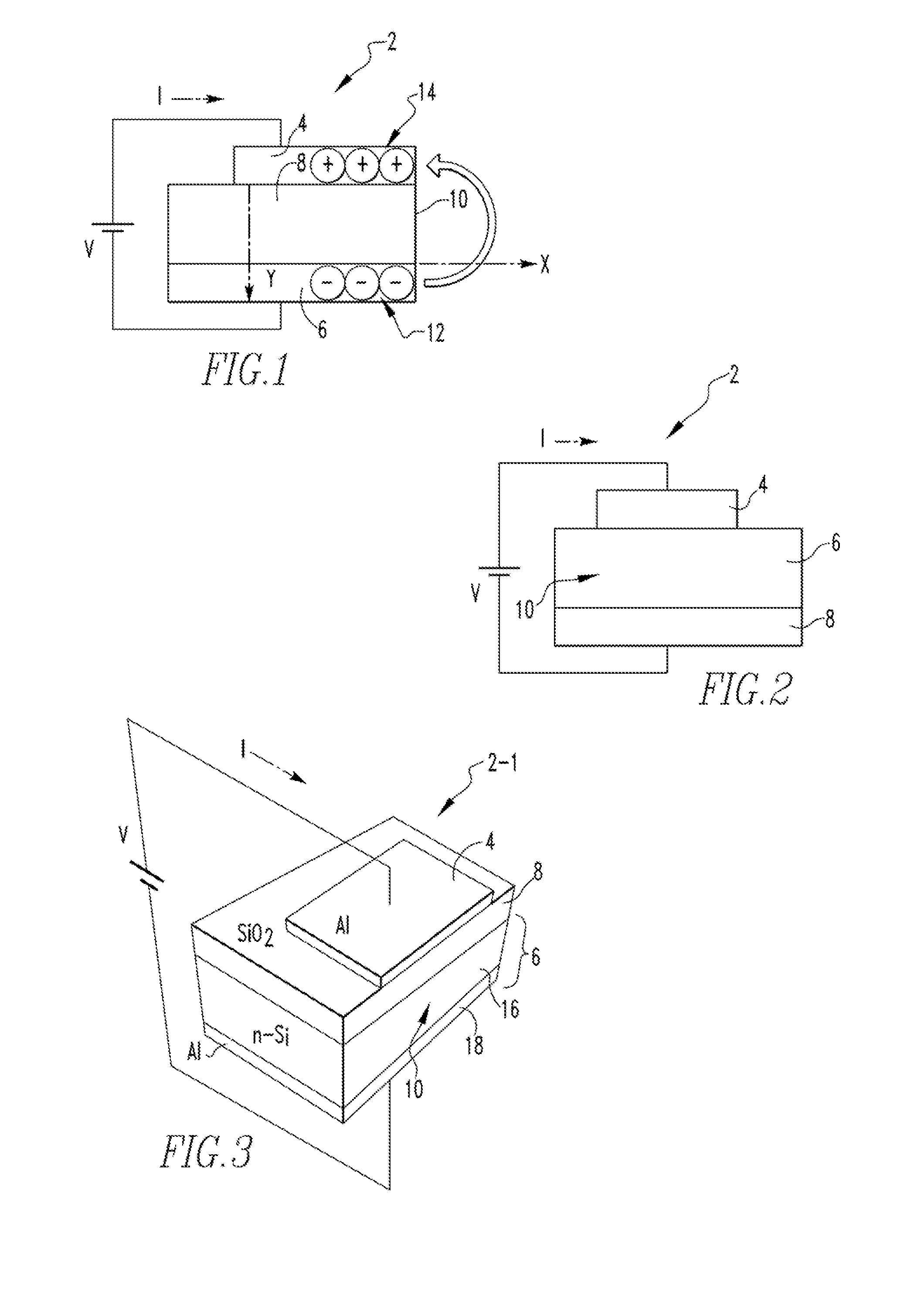
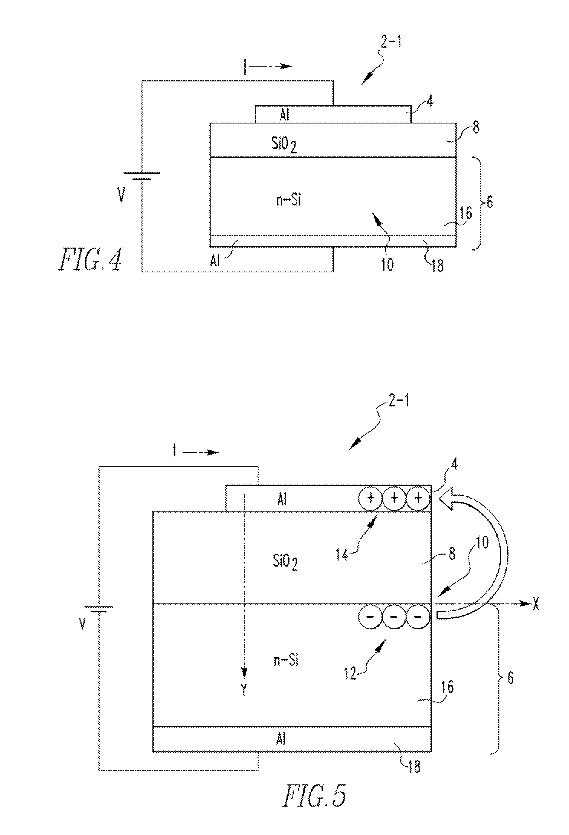
The patent describes various electronic devices that have a structure with a first conducting layer, a second conducting layer, and an insulating layer, and at least one side wall that extends from the insulating layer to the second conducting layer. The side wall includes a portion of each of the first and second conducting layers and the insulating layer. When a bias voltage is applied between the first and second conducting layers, a two dimensional electron system is induced in the first and second conducting layers, and electrons from this system are emitted from the side wall as a result of Coulombic repulsion and travel in air. The technical effects of this structure include improved performance and efficiency of electronic devices, as well as improved sensing and detection capabilities.

Problems solved by technology

Achieving a ballistic transport of charge carriers in a solid-state medium, however, requires a careful design of materials and structure, because a high electric field applied across a channel often incurs numerous conflicting situations with a requisite scattering-free transport in the medium.

Method used


Image

  • Low voltage nanoscale vacuum electronic devices
  • Low voltage nanoscale vacuum electronic devices
  • Low voltage nanoscale vacuum electronic devices

Examples


Embodiment Construction

[0041]As used herein, the singular form of “a”, “an”, and “the” include plural references unless the context clearly dictates otherwise. As used herein, the statement that two or more parts or components are “coupled” shall mean that the parts are joined or operate together either directly or indirectly, i.e., through one or more intermediate parts or components, so long as a link occurs. As used herein, “directly coupled” means that two elements are directly in contact with each other. As used herein, “fixedly coupled” or “fixed” means that two components are coupled so as to move as one while maintaining a constant orientation relative to each other.

[0042]As used herein, the word “unitary” means a component is created as a single piece or unit. That is, a component that includes pieces that are created separately and then coupled together as a unit is not a “unitary” component or body. As employed herein, the statement that two or more parts or components “engage” one another shal...


PUM


Abstract

An electronic device including a first conducting layer, a second conducting layer, and an insulating layer provided between the conducting layers. At least one side wall extends from the first conducting layer to the second conducting layer and includes at least a portion of the first conducting layer, the second conducting layer and the insulating layer. A bias voltage is applied between the first and second conducting layers, wherein responsive to the bias voltage, a two dimensional electron system is induced at least in one of the first conducting layer and the second conducting layer, and wherein electrons from the two dimensional electron system are emitted from the side wall side wall as a result of Coulombic repulsion and travel in air from the one of the first conducting layer and the second conducting layer to the other of the first conducting layer and the second conducting layer.

Description

CROSS-REFERENCE TO RELATED APPLICATIONS[0001]This application is a divisional of U.S. patent application Ser. No. 13 / 888,493, entitled “Low Voltage Nanoscale Vacuum Electronic Devices” and filed on May 7, 2013, which application claims priority under 35 U.S.C. §119(e) from provisional U.S. patent application No. 61 / 644,768, entitled “Low Voltage Nanoscale Vacuum Electronic Devices” and filed on May 9, 2012, the contents of which are incorporated herein by reference.GOVERNMENT CONTRACT[0002]This invention was made with government support under NSF Grant #ECCS-0925532 awarded by the National Science Foundation. The government has certain rights in the invention.BACKGROUND OF THE INVENTION[0003]1. Field of the Invention[0004]The present invention pertains to low voltage, high speed nano-vacuum electronic devices, and, in particular, the device structure wherein Coulombic repulsion in a two-dimensional electron system induced in a cathode of the electronic device is used to enable thres...

Claims


Application Information

Patent Timeline
Patent Type & Authority Applications(United States)
IPC IPC(8): H01J1/304H01L31/0224H01L31/101H01L27/146H01J19/24H01L31/062
CPCH01J1/3046H01J19/24H01L31/022466H01L31/101H01L27/146H01L31/062H01L29/66181H01L29/94H01L31/06H01L31/08H01L31/113H01L27/1446Y02E10/50H01L29/7613H01L29/66439H01J3/022H01J2201/30423H01J1/3042
Inventor KIM, HONG KOOSRISONPHAN, SIWAPON
Owner UNIV OF PITTSBURGH OF THE COMMONWEALTH SYST OF HIGHER EDUCATION
Why Eureka
Try Eureka