Electronic Device, Pressure Sensor, Altimeter, Electronic Apparatus, and Moving Object

a technology of electronic equipment and moving objects, applied in the direction of microstructural equipment, fluid speed measurement, instruments, etc., can solve the problems of easy collapse of the first covering layer and the second covering layer, cracking of the second metal layer, etc., to achieve excellent reliability

Inactive Publication Date: 2016-07-28
SEIKO EPSON CORP
View PDF5 Cites 0 Cited by
  • Summary
  • Abstract
  • Description
  • Claims
  • Application Information

AI Technical Summary

Benefits of technology

[0033]With this configuration, it is possible to provide a moving object having excellent reliability.

Problems solved by technology

However, in the electronic device disclosed in JP-A-2013-45893, via wiring is disposed between the first metal layer and the second metal layer, and therefore, there is a problem in that a step is formed in accordance with the shape of the via wiring in the second metal layer (the first covering layer) and the step causes the occurrence of cracking of the second metal layer.
For example, when a change in air pressure occurs, or the like, stress concentrates on the step of the second metal layer and thus cracking occurs in the second metal layer.
If cracking occurs in the second metal layer, the collapse of the first covering layer and the second covering layer easily occurs, or a problem such as vacuum leakage of the cavity portion or the insufficient strength of the surrounding wall occurs due to the infiltration of an etching solution into an unwilling place when forming the cavity portion by etching through the through-hole of the first covering layer.
Further, when forming the internal space by such etching, if a step or cracking occurs in the covering layer, an etching solution infiltrates into an unwilling place, and thus a problem such as vacuum leakage of the internal space or the insufficient strength of the wall section occurs.
When being within such a range of the value of A / B, the covering layer easily collapses, and if a step occurs in the covering layer, cracking easily occurs in the covering layer.

Method used


Image

  • Electronic Device, Pressure Sensor, Altimeter, Electronic Apparatus, and Moving Object
  • Electronic Device, Pressure Sensor, Altimeter, Electronic Apparatus, and Moving Object
  • Electronic Device, Pressure Sensor, Altimeter, Electronic Apparatus, and Moving Object

Examples


first embodiment

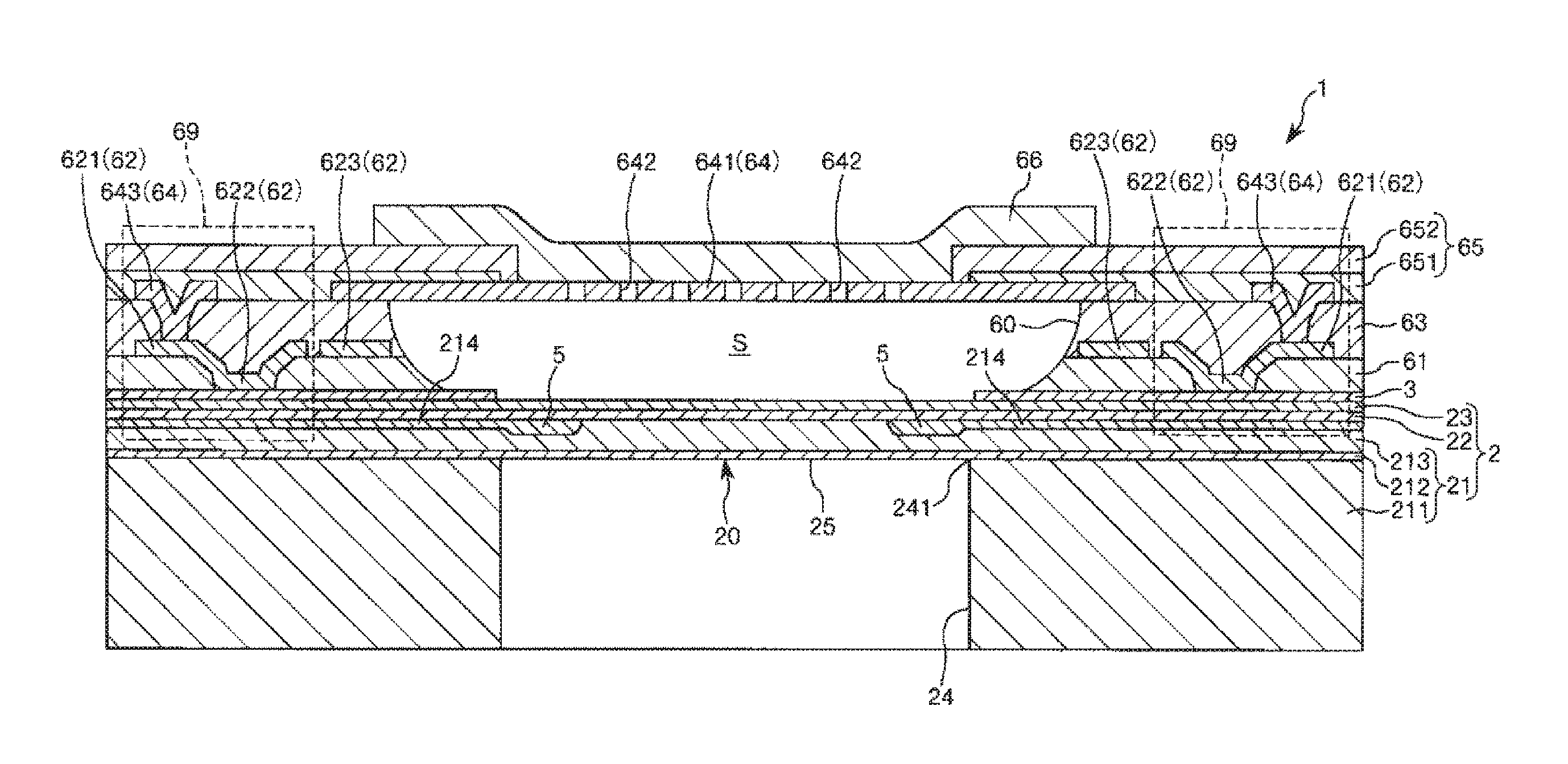
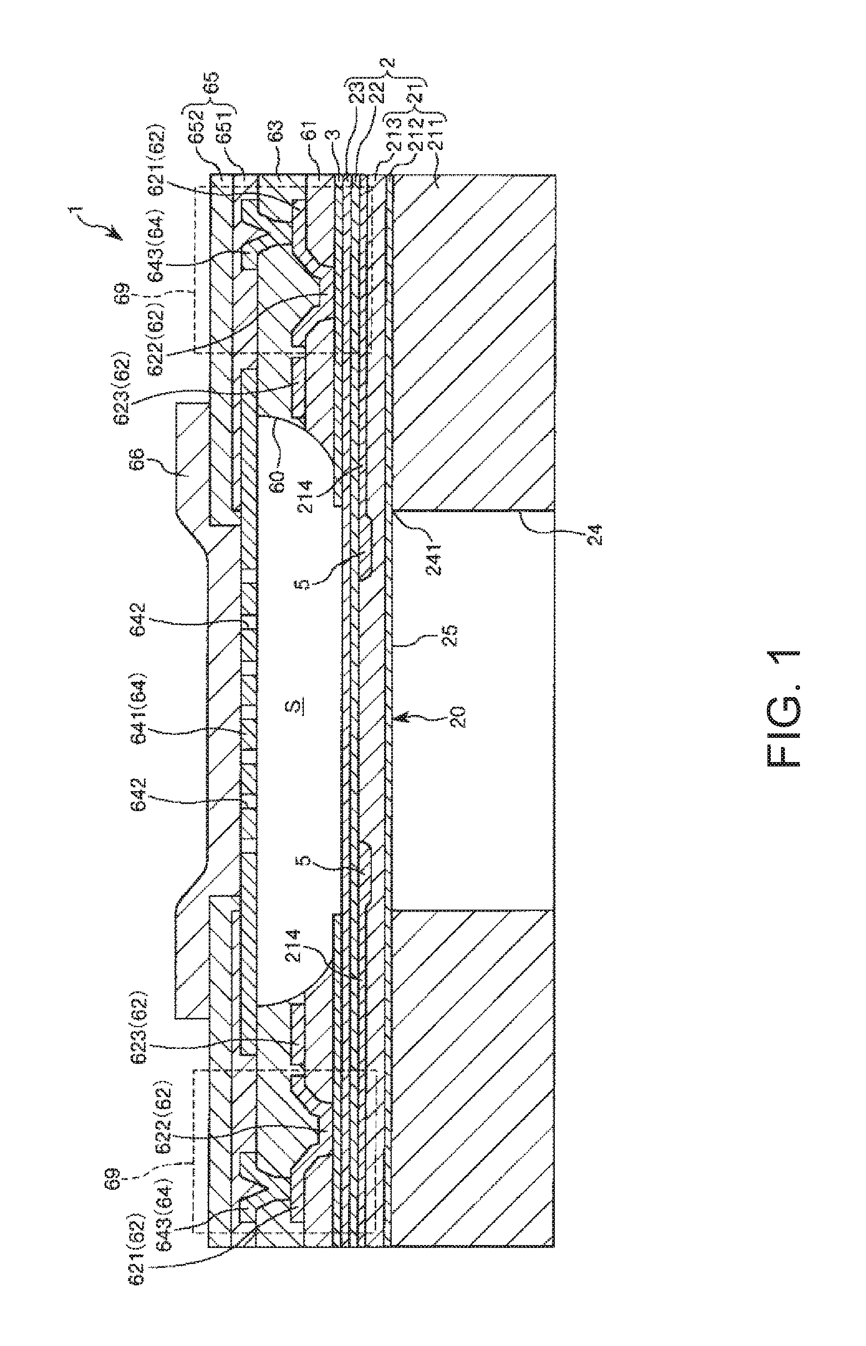
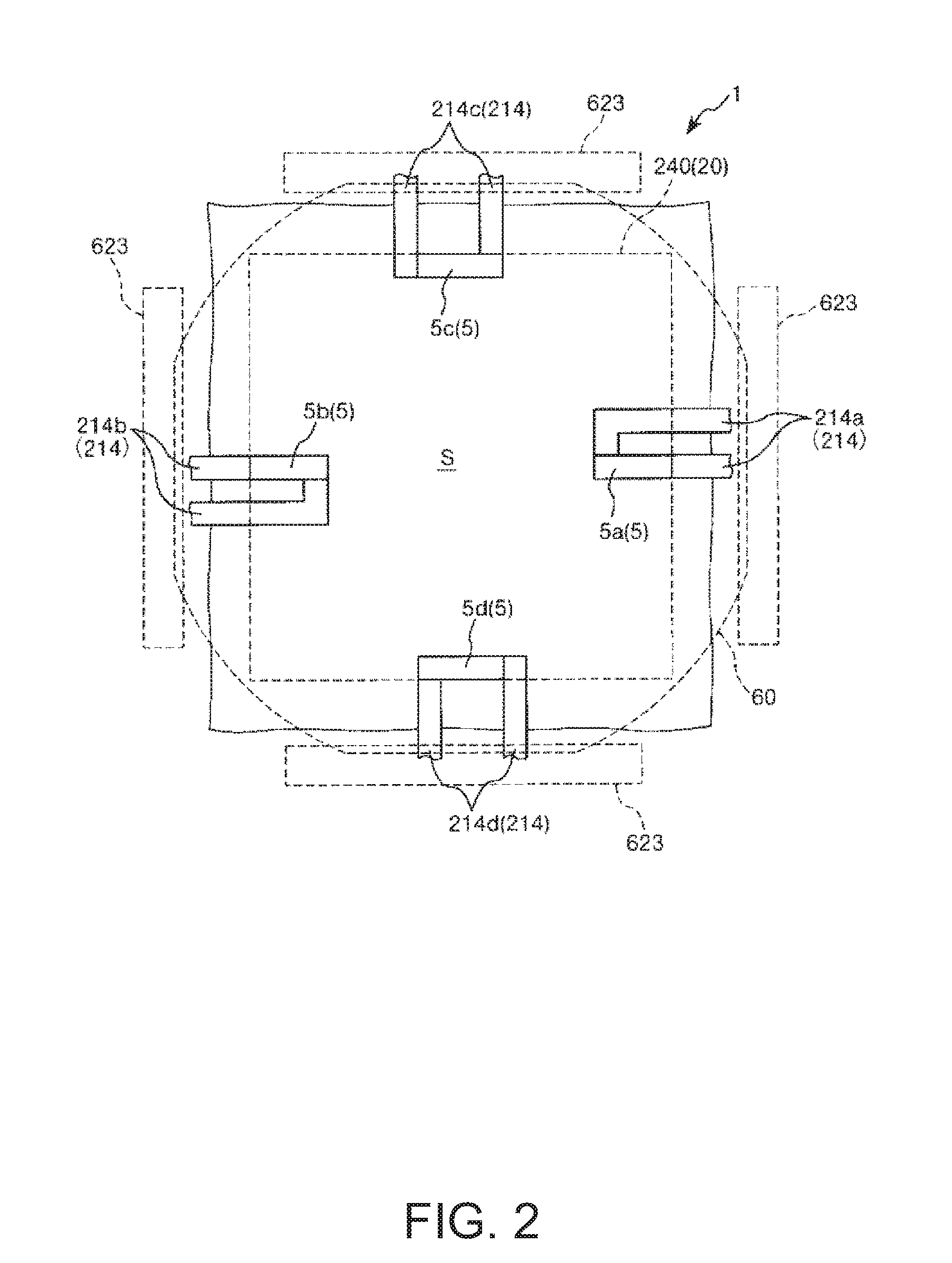
[0050]FIG. 1 is a cross-sectional view showing an electronic device (a physical quantity sensor) according to a first embodiment of the invention. FIG. 2 is a plan view showing the disposition of a piezoresistive element (a sensor element) and a wall section of the physical quantity sensor shown in FIG. 1. FIGS. 3A and 3B are diagrams for describing an operation of the physical quantity sensor shown in FIG. 1, in which FIG. 3A is a cross-sectional view showing a pressurization state and FIG. 3B is a plan view showing a pressurization state. In addition, in the following, for convenience of description, the upper side in FIG. 1 is referred to as a “top” and the lower side is referred to as a “bottom”.

[0051]A physical quantity sensor 1 which is the electronic device shown in FIG. 1 is provided with a substrate 2 having a diaphragm portion 20, a plurality of piezoresistive elements 5 (sensor elements) that are functional elements which are disposed at the diaphragm portion 20, a lamina...

second embodiment

[0129]Next, a second embodiment of the invention will be described.

[0130]FIG. 7 is a cross-sectional view showing an electronic device (a physical quantity sensor) according to a second embodiment of the invention. FIG. 8 is a plan view showing the disposition of a piezoresistive element (a sensor element) and a wall section of the physical quantity sensor shown in FIG. 7.

[0131]Hereinafter, the second embodiment of the invention will be described. However, a description is made focusing on differences from the embodiment described above, and with respect to the same matters, a description thereof is omitted.

[0132]This embodiment is the same as the first embodiment described above, except that the configuration of a wiring layer is different.

[0133]A physical quantity sensor 1A (an electronic device) shown in FIG. 7 is the same as the physical quantity sensor 1 of the first embodiment described above, except that the guard portion 623 is omitted and accordingly, the shape in a plan vi...

third embodiment

[0136]Next, a third embodiment of the invention will be described.

[0137]FIG. 9 is a cross-sectional view showing an electronic device (a vibrator) according to the third embodiment of the invention. FIGS. 10A and 10B are diagrams for describing a resonator with which the vibrator shown in FIG. 9 is provided, in which FIG. 10A is a cross-sectional view and FIG. 10B is a plan view.

[0138]Hereinafter, the third embodiment of the invention will be described. However, a description is made focusing on differences from the embodiment described above, and with respect to the same matters, a description thereof is omitted.

[0139]This embodiment is the same as the first embodiment described above, except that the electronic device according to the invention is applied to a vibrator.

[0140]An electronic device 1B shown in FIG. 9 has the same configuration as the physical quantity sensor 1 of the first embodiment described above, except that the electronic device 1B is provided with a substrate 2...


PUM


Abstract

An electronic device includes: a substrate; a piezoresistive element which is disposed on the side of the surface on one side of the substrate; a wall section which is disposed to surround the piezoresistive element in a plan view of the substrate, on the side of the surface on one side of the substrate; via wiring which is disposed on the side of the surface on one side of the substrate; and a covering layer which is disposed away from the via wiring in the plan view on the side opposite to the substrate with respect to the wall section and configures a cavity portion along with the substrate and the wall section.

Description

CROSS REFERENCE[0001]This application claims the benefit of Japanese Application No. 2015-013014, filed on Jan. 27, 2015. The disclosure of the prior application is hereby incorporated by reference herein in its entirety.BACKGROUND[0002]1. Technical Field[0003]The present invention relates to an electronic device, a pressure sensor, an altimeter, an electronic apparatus, and a moving object.[0004]2. Related Art[0005]An electronic device having a cavity portion formed by using a semiconductor manufacturing process is known (refer to, for example, JP-A-2013-45893). As an example of such an electronic device, for example, an electronic device disclosed in JP-A-2013-45893 is given, and the electronic device includes a substrate, a functional element disposed above the substrate, and a covering structure which defines a cavity portion in which the functional element is accommodated, and the covering structure has a first covering layer which has a through-hole communicating with the cavi...

Claims


Application Information

Patent Timeline
Patent Type & Authority Applications(United States)
IPC IPC(8): B81B7/00
CPCB81B7/007B81B2207/095B81B2203/0127B81B2201/0264B81C1/00182B81B2207/07
Inventor TANAKA, NOBUYUKI
Owner SEIKO EPSON CORP
Why Eureka
Try Eureka