

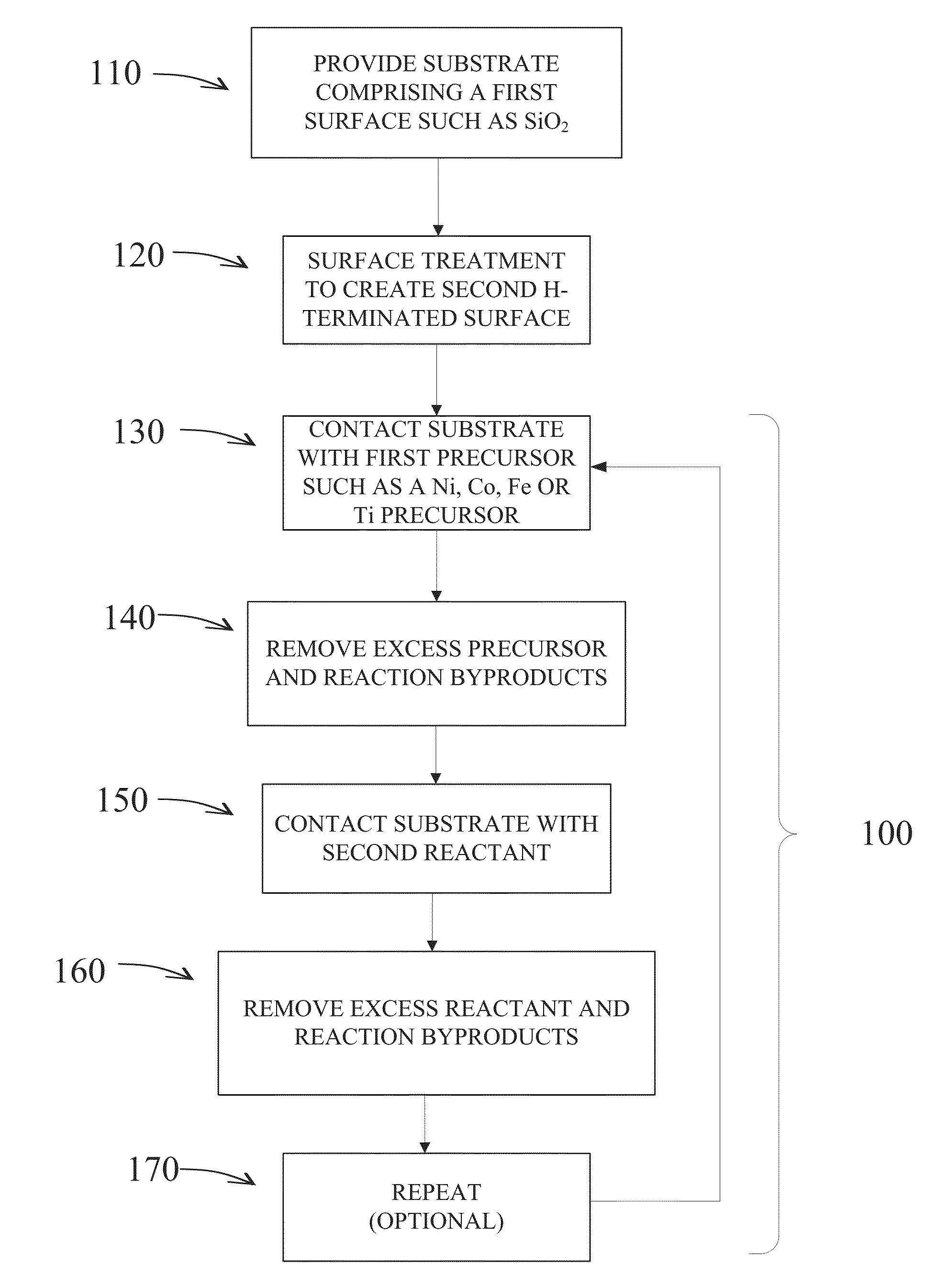
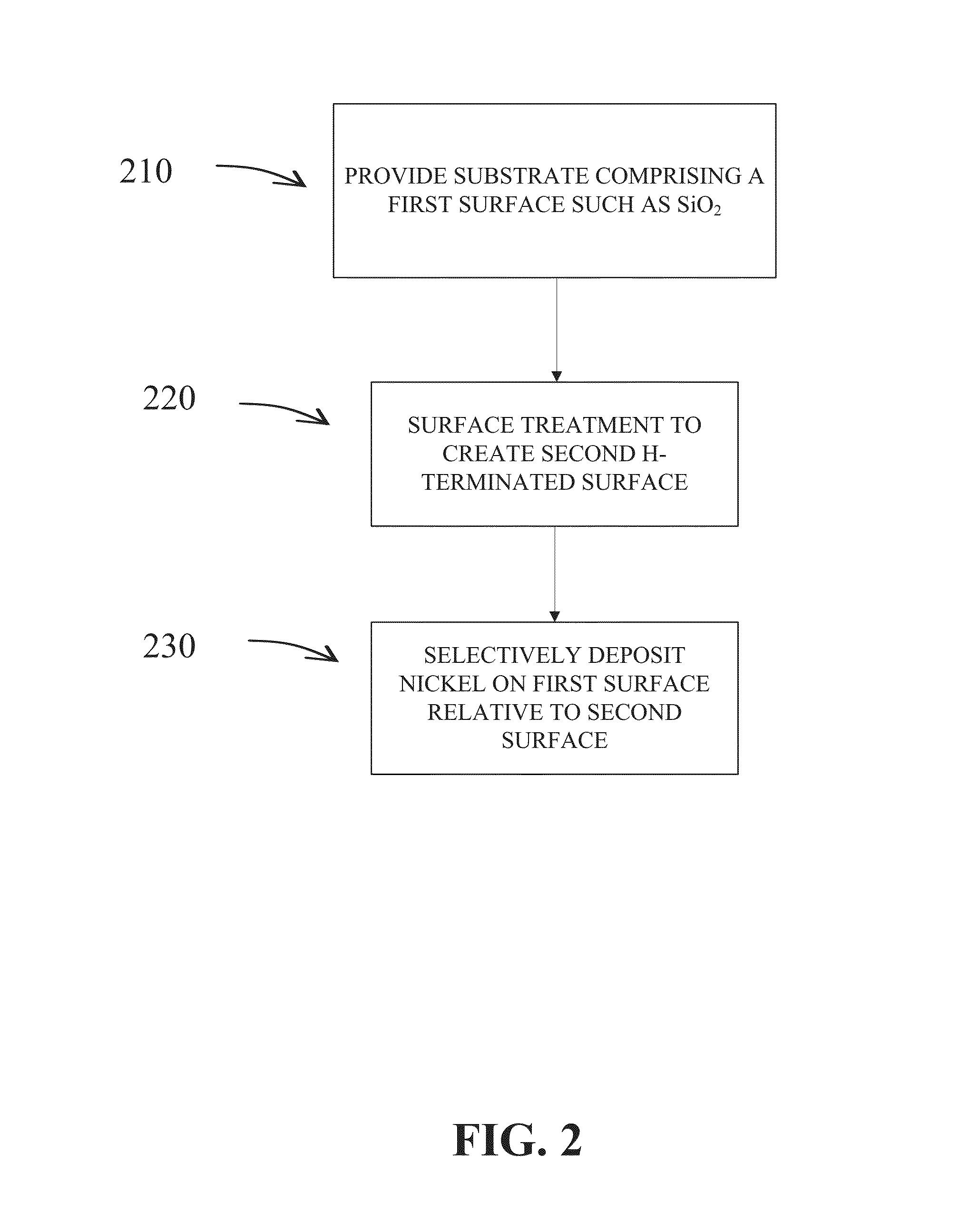
Selective deposition
a technology of selective deposition and vapor deposition process, which is applied in the direction of chemical vapor deposition coating, metal material coating process, coating, etc., can solve the problem of difficult to achieve selective deposition by vapor deposition process such as atomic layer deposition (ald)
- Summary
- Abstract
- Description
- Claims
- Application Information
AI Technical Summary
Benefits of technology
Problems solved by technology
Method used
Image

Examples
examples
[0195]The growth of Ni and NixNy was studied in both F-120 and Pulsar® 2000 reactors. Two coupon substrates (5×5 cm2) were loaded in an F-120 reactor simultaneously. The test was performed with a first substrate comprising a first SiO2 surface and a second HF etched Si surface, and a second substrate comprising an HF etched Si surface in the same deposition run. The first substrate comprising a SiO2 surface was masked and etched with HF to form a first SiO2 surface 710 and a second H-terminated surface 720. The reaction temperature was set to 300° C. and Ni was grown by a pulsed CVD process as described herein, using bis(4-N-ethylamino-3-penten-2-N-ehtyliminato nickel (II) as a Ni precursor. The CVD process included 1500 pulse and purge steps. No second reactant was pulsed into the reaction chamber. As illustrated in FIG. 7, nickel was selectively deposited on the first SiO2 surface 710 of the first substrate relative to the second HF etched (Si—H) surface 720. No nickel was deposit...
PUM
| Property | Measurement | Unit |
|---|---|---|
| thickness | aaaaa | aaaaa |
| thickness | aaaaa | aaaaa |
| temperature | aaaaa | aaaaa |
Abstract
Description
Claims
Application Information