Display panel

a display panel and panel technology, applied in the field of display panels, can solve the problems of affecting the aperture ratio of the product, difficult assembly precision control, and high resolution usually achieved at the cost of the aperture ratio of the pixel, so as to achieve the effect of increasing the aperture ratio of the display panel and reducing the area of the light-shielding matrix

Active Publication Date: 2016-08-11
INNOLUX CORP
View PDF3 Cites 8 Cited by
  • Summary
  • Abstract
  • Description
  • Claims
  • Application Information

AI Technical Summary

Benefits of technology

[0008]The invention is directed to a display panel. According to some embodiments, through the design of disposing a metal layer and an anti-reflection structure on a substrate, the area of the light-shielding matrix can be reduced and the aperture ratio of the display panel can be effectively increased.

Problems solved by technology

However, high resolution is usually achieved at the cost of aperture ratio of the pixel.
When the elements on the substrates may be changed, rotated or deformed during the assembly process, the assembly precision will be hard to control and the aperture ratio of the product will be affected.

Method used


Image

  • Display panel
  • Display panel
  • Display panel

Examples


first embodiment

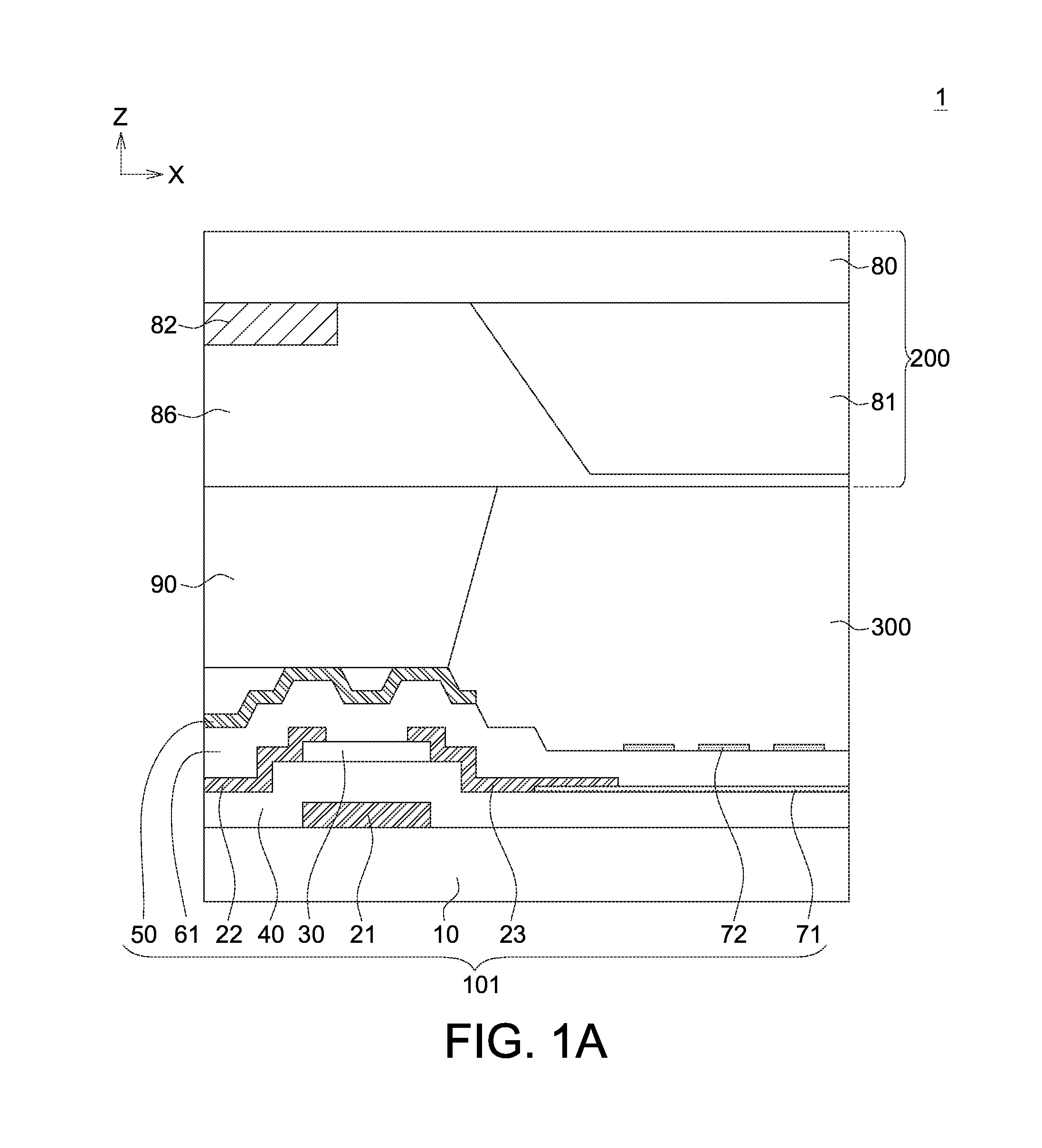
[0026]FIG. 1A is a partial cross-sectional view of a display panel 1 according to the first embodiment of the present invention. FIG. 1B is a partial top view of the display panel 1 according to the first embodiment of the present invention. Here, FIG. 1A is a cross-sectional view of the display panel 1 viewed along a cross-sectional line A-A′ of FIG. 1B.

[0027]As indicated in FIGS. 1A and 1B, the display panel 1 may include a first substrate 101, a second substrate 200 and a display medium 300. The second substrate 200 and the first substrate 101 are disposed oppositely. The display medium 300 is disposed between the first substrate 101 and the second substrate 200. The display medium 300 can be realized by such as a liquid crystal layer or an organic light emitting layer. Besides, the display panel 1 may also include a spacer 90 disposed between the first substrate 101 and the second substrate 200.

[0028]In the first embodiment of the present invention, the first substrate 101 inclu...

second embodiment

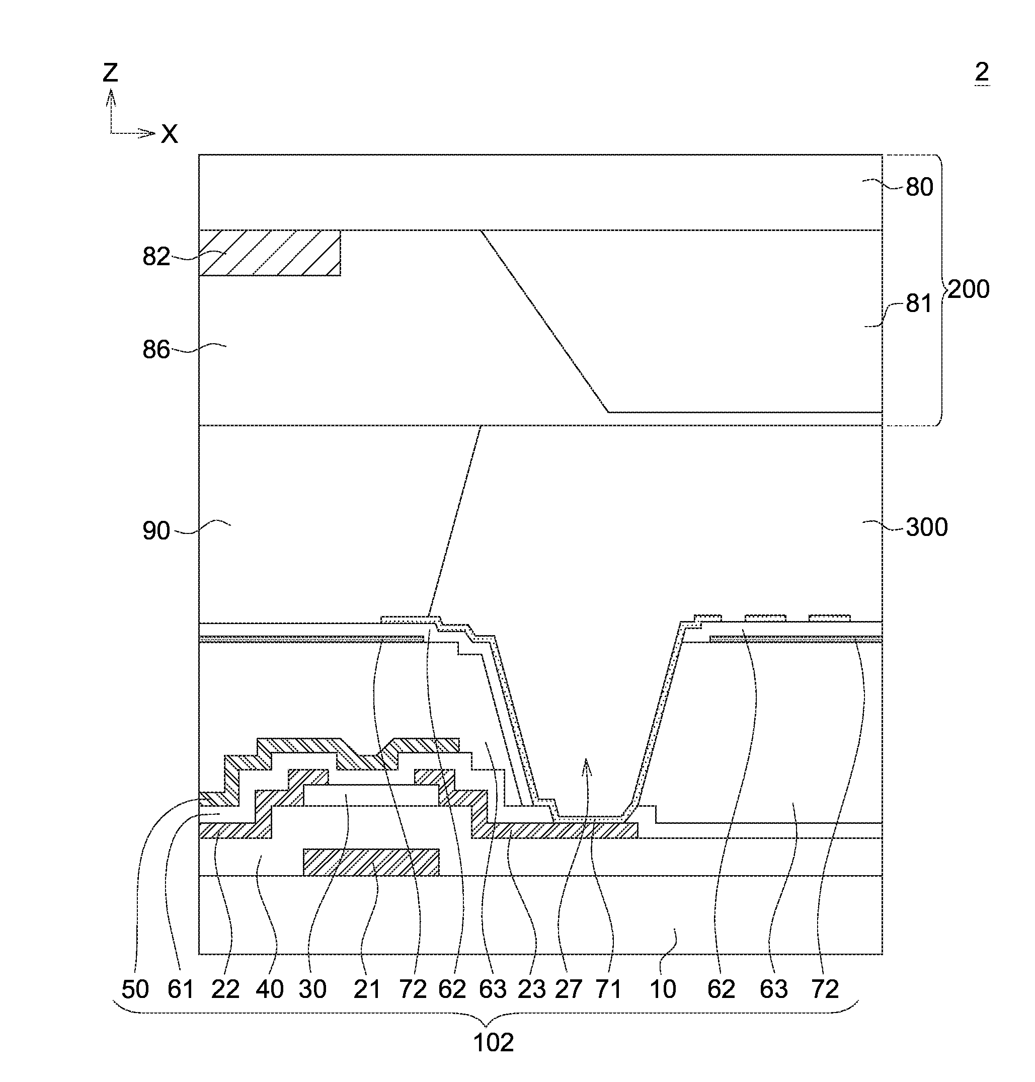
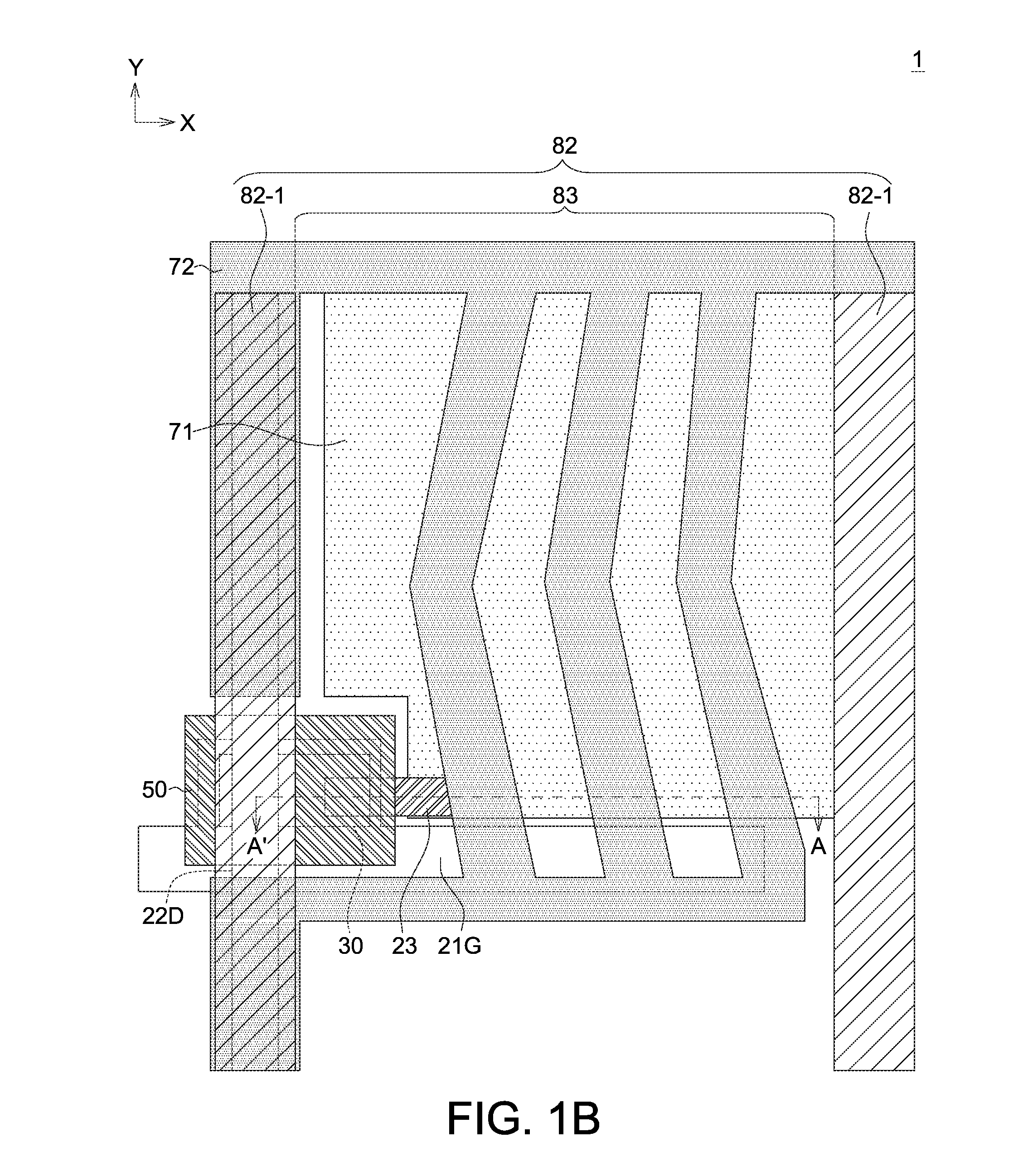
[0043]FIG. 3A is a partial cross-sectional view of a display panel 2 according to the second embodiment of the present invention. FIG. 3B is a partial top view of a display panel 2 according to the second embodiment of the present invention. Here, FIG. 3A is a cross-sectional view of the display panel 1 viewed along a cross-sectional line B-B′ of FIG. 3B. It should be noted that in order to more clearly illustrate the structure of the display panel 2, some elements such as the data line 22D and the gate line 21G are omitted in FIG. 3B.

[0044]Like the first embodiment, the display panel 2 may include a first substrate 102, a second substrate 200 and a display medium 300. The second substrate 200 and the first substrate 102 are disposed oppositely. The display medium 300 is disposed between the first substrate 102 and the second substrate 200. Moreover, the display panel 2 may also include a spacer 90 disposed between the first substrate 102 and the second substrate 200. The display pa...

third embodiment

[0052]FIG. 4 is a partial cross-sectional view of a display panel 3 according to the third embodiment of the present invention. In the present invention, the top view of the display panel 3 of the third embodiment is similar to that of the second embodiment, and the structure may be disclosed with reference to FIG. 3B.

[0053]Like the second embodiment, the display panel 3 may include a first substrate 103, a second substrate 200 and a display medium 300. The second substrate 200 and the first substrate 103 are disposed oppositely. The display medium 300 is disposed between the first substrate 103 and the second substrate 200. Besides, the display panel 3 may also include a spacer 90 disposed between the first substrate 103 and the second substrate 200. The display panel 3 of the present embodiment is different from the display panel 2 of the second embodiment in the shielding structure 50 of the first substrate 103.

[0054]In the present embodiment, the shielding structure 50 may have ...


PUM

PropertyMeasurementUnit
light-shieldingaaaaaaaaaa
anti-reflection structureaaaaaaaaaa
sizesaaaaaaaaaa

Abstract

A display panel including a first substrate, a second substrate and a display medium is provided. The first substrate includes a base substrate, a gate, an active layer, a source, a drain, and a shielding structure. The gate is disposed on the base substrate. The active layer is electrically insulated from and disposed correspondingly to the gate. The source and the drain are electrically connected to the active layer. The shielding structure is disposed on the active layer and covers at least part of the active layer. The shielding structure includes a metal layer and an anti-reflection structure. The display medium is disposed between the first substrate and the second substrate.

Description

[0001]This application claims the benefit of Taiwan application Serial No. 104104282, filed Feb. 9, 2015, the subject matter of which is incorporated herein by reference.BACKGROUND OF THE INVENTION[0002]1. Field of the Invention[0003]The invention relates in general to a display panel, and more particularly to a display panel with high aperture ratio.[0004]2. Description of the Related Art[0005]Along with the rapid development in display technology, high resolution display capable of processing digital signals and showing more delicate frames has gradually become a mainstream product in the market for whatever panel sizes. That is, the same size requires more pixels.[0006]However, high resolution is usually achieved at the cost of aperture ratio of the pixel. Here, the aperture ratio refers to the ratio of light transmissive area to the entire area of the pixel. The light transmissive area refers to the area of the pixel exclusive of wires and transistors. The higher the aperture ra...

Claims


Application Information

Patent Timeline
Patent Type & Authority Applications(United States)
IPC IPC(8): H01L27/12G02F1/1335G02F1/1362G02F1/1368
CPCH01L27/124G02F1/1368G02F2001/133357G02F1/136227G02F1/133502G02F1/133512H01L29/78633G02F1/1362G02F1/136218G02F1/134318G02F1/134372H10K59/126H10K59/1213G02F1/134309G02F1/136209G02F2201/121G02F2201/123
Inventor LAI, HSIAO-PINGLU, CHAO-LIANGYAN, TZU-MINHSIEH, TSAU-HUA
Owner INNOLUX CORP
Why Eureka
Try Eureka