Liquid Crystal Display Array Substrate and Related Liquid Crystal Display

a liquid crystal display and array substrate technology, applied in non-linear optics, instruments, optics, etc., can solve problems such as abnormal charging of pixels, and achieve the effects of reducing the parasitic capacitance of data lines and common electrode lines on the array substrate, reducing the number of data lines/common electrode lines, and reducing the delay on data lines

Inactive Publication Date: 2016-09-01
TCL CHINA STAR OPTOELECTRONICS TECH CO LTD
View PDF1 Cites 5 Cited by
  • Summary
  • Abstract
  • Description
  • Claims
  • Application Information

AI Technical Summary

Benefits of technology

[0031]In embodiments of the present invention, pixel structures deployed on an array substrate are arranged in plural rows along extension of data lines, and two adjacent rows of pixel structures are arranged in opposition in sequence, therefore two adjacent rows of pixel structures with two gates lines remote to each other share the common electrode line. As a result, chances of data lines and common electrode lines crossing to each other on the array substrate are reduced, therefore number of data lines / common electrode lines parasitic capacitances is reduced; RC delay on data lines decreases, and charging rate of the pixel increases.

Problems solved by technology

The defect of the prior art is that parasitic capacitances cause resistance-capacitance (RC) delay and signal distortion on the data line, resulting in pixel abnormal charging (such as insufficient or erroneous charging).

Method used


Image

  • Liquid Crystal Display Array Substrate and Related Liquid Crystal Display
  • Liquid Crystal Display Array Substrate and Related Liquid Crystal Display
  • Liquid Crystal Display Array Substrate and Related Liquid Crystal Display

Examples


Embodiment Construction

[0038]Spatially relative terms, such as “beneath”, “below”, “lower”, “above”, “upper” and the like, may be used herein for ease of description to describe one element or feature's relationship to another element(s) or feature(s) as illustrated in the figures. It will be understood that the spatially relative terms are intended to encompass different orientations of the device in use or operation in addition to the orientation depicted in the figures.

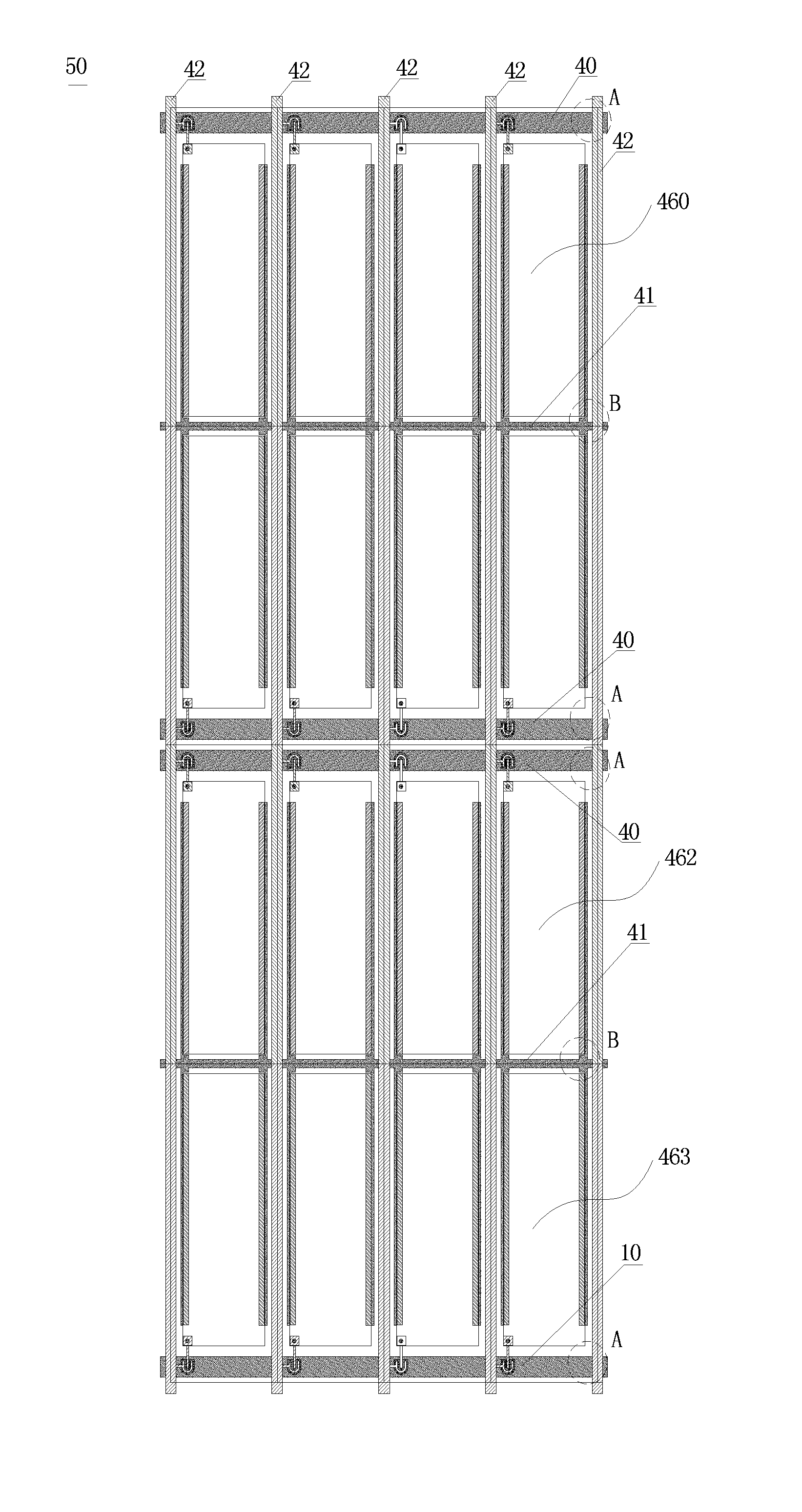
[0039]FIG. 3 is a structural diagram of pixel structures on a liquid crystal display (LCD) array substrate of the present invention. A pixel structure 460 is formed on a substrate, whereas the pixel structure 460 is a zone formed by crossing of two adjacent data lines 42, a gate line 40 and a common electrode line 41. The data lines 42 send signals to pixels, the gate line 40 sends scan signals, the common electrode line 41 provides common voltage to the pixels.

[0040]In detail, the pixel structure 46 comprises:

[0041]the gate line 40 and ...


PUM

PropertyMeasurementUnit
widthaaaaaaaaaa
sizeaaaaaaaaaa
parasitic capacitancesaaaaaaaaaa

Abstract

An array substrate used in an LCD is provided. The array substrate includes: a substrate and pixel structures formed on the substrate. Each pixel structure includes: a gate line and a common electrode line formed by the same metal layer on the substrate, two data lines above and crossing the gate line and the common electrode line, a TFT electrically connected to the two data lines and the gate line, a pixel electrode electrically connected to the TFT and deployed between the gate line and the common electrode line. The pixel structures are arranged in a plurality of rows along an extension of the data lines. Two adjacent rows of the pixel structures are arranged in opposite direction in sequence, and at least two adjacent rows of the pixel structures share the common electrode line. The LCD using the array substrate has lower RC delay on data lines, not only improving charging rate of pixel but also reducing cost of additional lines.

Description

CROSS-REFERENCE TO RELATED APPLICATION[0001]This application claims priority from and the benefit under 35 U.S.C. §119(a) of Chinese Patent Application No. 201310753035.8, filed on Dec. 31, 2013, which is hereby incorporated by reference for all purposes as if fully set forth herein.BACKGROUND OF THE INVENTION[0002]1. Field of the Invention[0003]The present invention relates to a thin film transistor liquid crystal display (TFT-LCD) field, more particularly, to a liquid crystal display (LCD) array substrate and a related LCD.[0004]2. Description of the Prior Art[0005]Driving circuits of TFT-LCD usually comprise indispensible components such as gate lines, data lines, thin film transistor (TFT) and common electrode lines (Com). In conventional photo-etching art, gate and common electrode line are usually formed by the same metal layer.[0006]FIG. 1 is a diagram of a pixel structure on a conventional liquid crystal display (LCD) array substrate. The pixel structure is formed on the arr...

Claims


Application Information

Patent Timeline
Patent Type & Authority Applications(United States)
IPC IPC(8): G02F1/1362G02F1/1343G02F1/1368G02F1/1335
CPCG02F1/136286G02F1/133514G02F2001/13606G02F1/1368G02F1/13439G02F1/136213G02F1/13606G02F1/136218
Inventor ZHENG, HUA
Owner TCL CHINA STAR OPTOELECTRONICS TECH CO LTD
Why Eureka
Try Eureka