Digital-To-Analog Converter Using Nonlinear Capacitance Compensation

a digital-to-analog converter and nonlinear capacitance compensation technology, applied in the direction of digital-analog convertors, electronic switching, pulse techniques, etc., can solve the problems of parasitic capacitance, unwanted capacitance, affecting the linearity of electronic devices,

Active Publication Date: 2016-09-01
AVAGO TECH INT SALES PTE LTD
View PDF0 Cites 5 Cited by
  • Summary
  • Abstract
  • Description
  • Claims
  • Application Information

AI Technical Summary

Problems solved by technology

However, in practice, the semiconductor fabrication process often introduces unwanted capacitances, often referred to as parasitic capacitances, into the transistors as well as the interconnections between these transistors.
These parasitic capacitances can affect the linearity of the electronic device.
However, in practice, the parasitic capacitances of the transistors of the DAC often introduce non-linearities into the DAC causing the analog output signal to no longer be directly proportional to the digital input signal making the analog output signal less predictable.

Method used


Image

  • Digital-To-Analog Converter Using Nonlinear Capacitance Compensation
  • Digital-To-Analog Converter Using Nonlinear Capacitance Compensation
  • Digital-To-Analog Converter Using Nonlinear Capacitance Compensation

Examples


Embodiment Construction

[0018]Overview

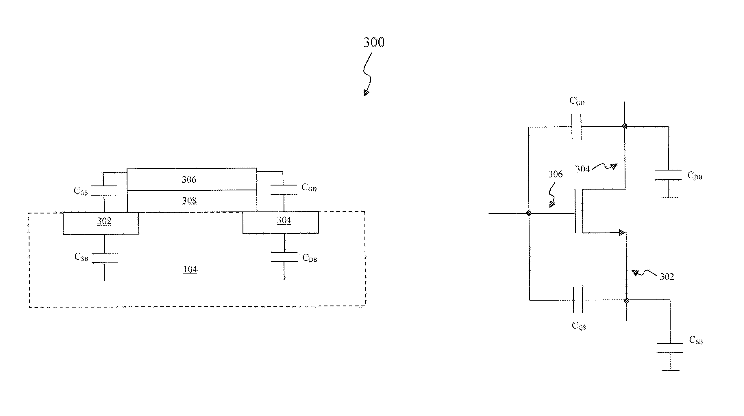
[0019]A semiconductor device fabrication operation is commonly used to manufacture one or more integrated circuits onto a semiconductor substrate. The semiconductor device fabrication operation forms one or more transistors onto an arrangement of fabrication layers to form the one or more integrated circuits which introduces unwanted capacitances, often referred to as parasitic capacitances, into the one or more transistors. The various systems and methods disclosed herein include one or more compensation modules that, when combined with the parasitic capacitances of the one or more transistors, ideally linearizes the non-linearity caused by the parasitic capacitances of the one or more transistors. For example, the compensation module of the present disclosure incorporates a non-linear or a piecewise linear transfer function that is inversely related to the parasitic capacitances of the one or more transistors.

[0020]Integrated Circuit

[0021]FIG. 1 illustrates a schemat...


PUM


Abstract

A semiconductor device fabrication operation is commonly used to manufacture one or more integrated circuits onto a semiconductor substrate. The semiconductor device fabrication operation forms one or more transistors onto an arrangement of fabrication layers to form the one or more integrated circuits which introduces unwanted capacitances, often referred to as parasitic capacitances, into the one or more transistors. The one or more integrated circuits include one or more compensation modules that, when combined with the parasitic capacitances of the one or more transistors, ideally linearizes the non-linearity caused by the parasitic capacitances of the one or more transistors. For example, the one or more compensation modules incorporate a non-linear or a piecewise linear transfer function that is inversely related to the parasitic capacitances of the one or more transistors.

Description

CROSS-REFERENCE TO RELATED APPLICATIONS[0001]The present application claims the benefit of U.S. Provisional Patent Appl. No. 62 / 121,834, filed Feb. 27, 2015, which is incorporated herein by reference in its entirety.BACKGROUND[0002]1. Field of Disclosure[0003]The present disclosure generally relates to improving the linearity of an electronic circuit and including nonlinear capacitance compensation to improve the linearity of a digital-to-analog converter (DAC).[0004]2. Related Art[0005]The continued improvement of the semiconductor fabrication process has allowed manufacturers and designers to create smaller and more powerful electronic devices. These electronic devices have higher speed, more density, and consume less power than their predecessors. In its infancy, manufacturers and designers used a 10 μm semiconductor fabrication process while a 5 nm semiconductor fabrication process is contemplated in the future with the surface area of each node being halved every two years. The...

Claims


Application Information

Patent Timeline
Patent Type & Authority Applications(United States)
IPC IPC(8): H03M1/06H03K17/16H03M1/66
CPCH03M1/0604H03K17/165H03M1/66H03M1/742
Inventor WARD, CHRISTOPHERBULT, KLAASELUMALAI, INIYAVAN
Owner AVAGO TECH INT SALES PTE LTD
Why Eureka
Try Eureka