
Mask inspection apparatus and mask inspection method

a mask inspection and mask technology, applied in the field of mask inspection apparatus and mask inspection method, can solve the problems of large degradation factor of mask pattern, inability etc., to achieve high resolution, the effect of not being able to obtain accurate cd map and inability to accurately measure the line width of pattern

Active Publication Date: 2016-09-15
NUFLARE TECH INC
View PDF9 Cites 8 Cited by
  • Summary
  • Abstract
  • Description
  • Claims
  • Application Information

AI Technical Summary

Benefits of technology

The present invention relates to a mask inspection apparatus and method that can inspect a pattern on a mask to ensure it is properly formed. The apparatus includes an illumination optical unit, an imaging unit, a reference image data generating unit, a correcting unit, and a line width error obtaining unit. The method involves calibrating the sensor, acquiring optical image data of the pattern, correcting the gradation value of the optical image data, and obtaining the line width of the pattern. The technical effects of this invention include improved accuracy and efficiency in mask inspection.

Problems solved by technology

A defect of a mask pattern can be cited as a large factor of degradation in the production yield of a semiconductor element.
When a light quantity of the light source is fluctuated, a gradation value of the optical image data is fluctuated, and it is then impossible to accurately measure a line width of a pattern, and impossible to obtain an accurate CD map.
However, there is a problem in that the correction of the output fluctuation of the TDI sensor due to the light quantity fluctuation is not adequate, and a correction error occurs because of the difference between a band of a response frequency of the photodiode and a band of a response frequency of the TDI sensor.

Method used


Image

  • Mask inspection apparatus and mask inspection method
  • Mask inspection apparatus and mask inspection method
  • Mask inspection apparatus and mask inspection method

Examples


Embodiment Construction

[0020]The embodiments will now be described with reference to the accompanying drawings, wherein the same reference numerals designate corresponding or identical elements throughout the various drawings.

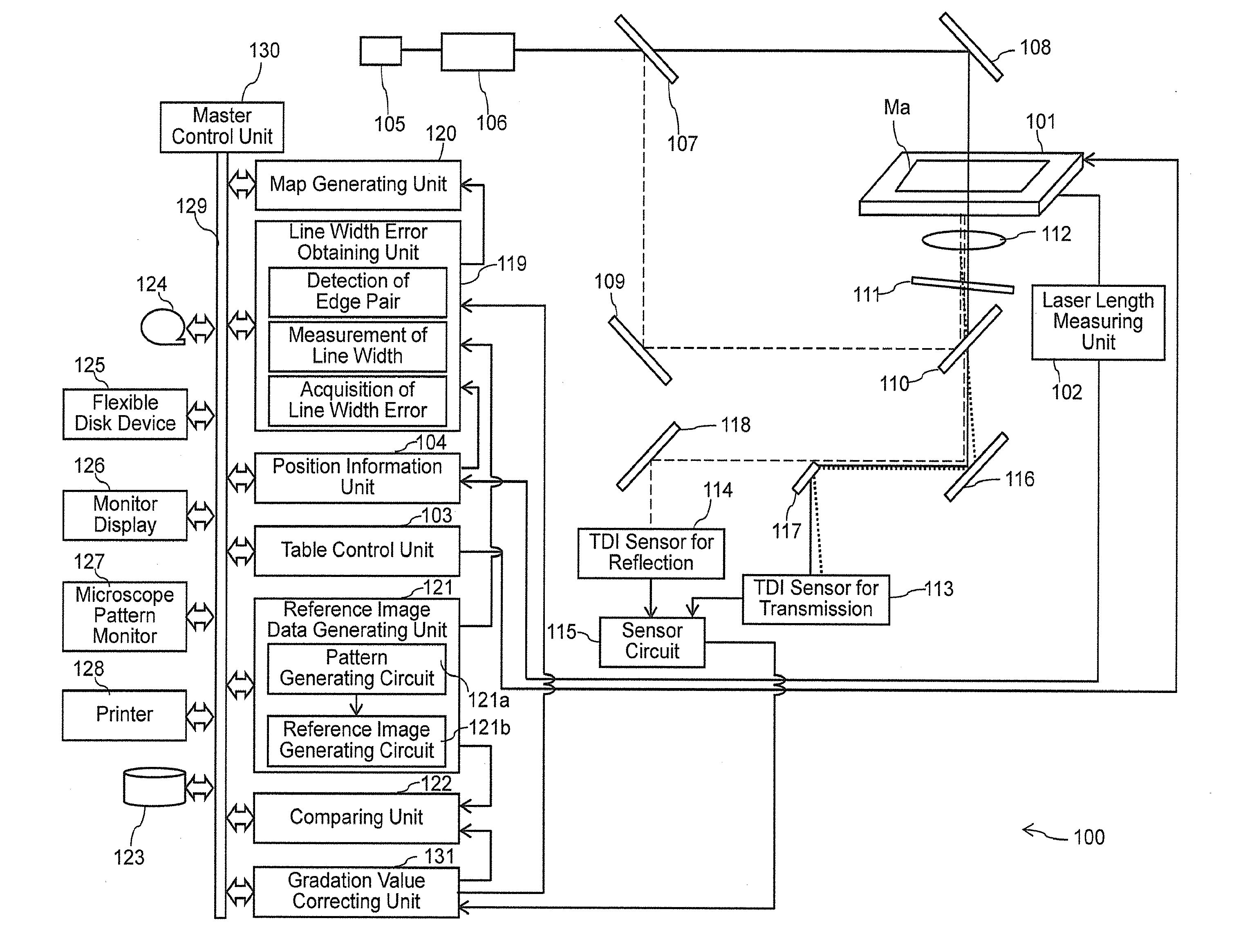
[0021]FIG. 1 is a schematic configuration diagram of a mask inspection apparatus 100 according to the present embodiment. The mask inspection apparatus 100 obtains optical image data of an inspection target, and then obtains a line width error (ΔCD) of the inspection target using the optical image data to generate a line width error map (ΔCD map). The main constituent components of the mask inspection apparatus 100 are as follows.

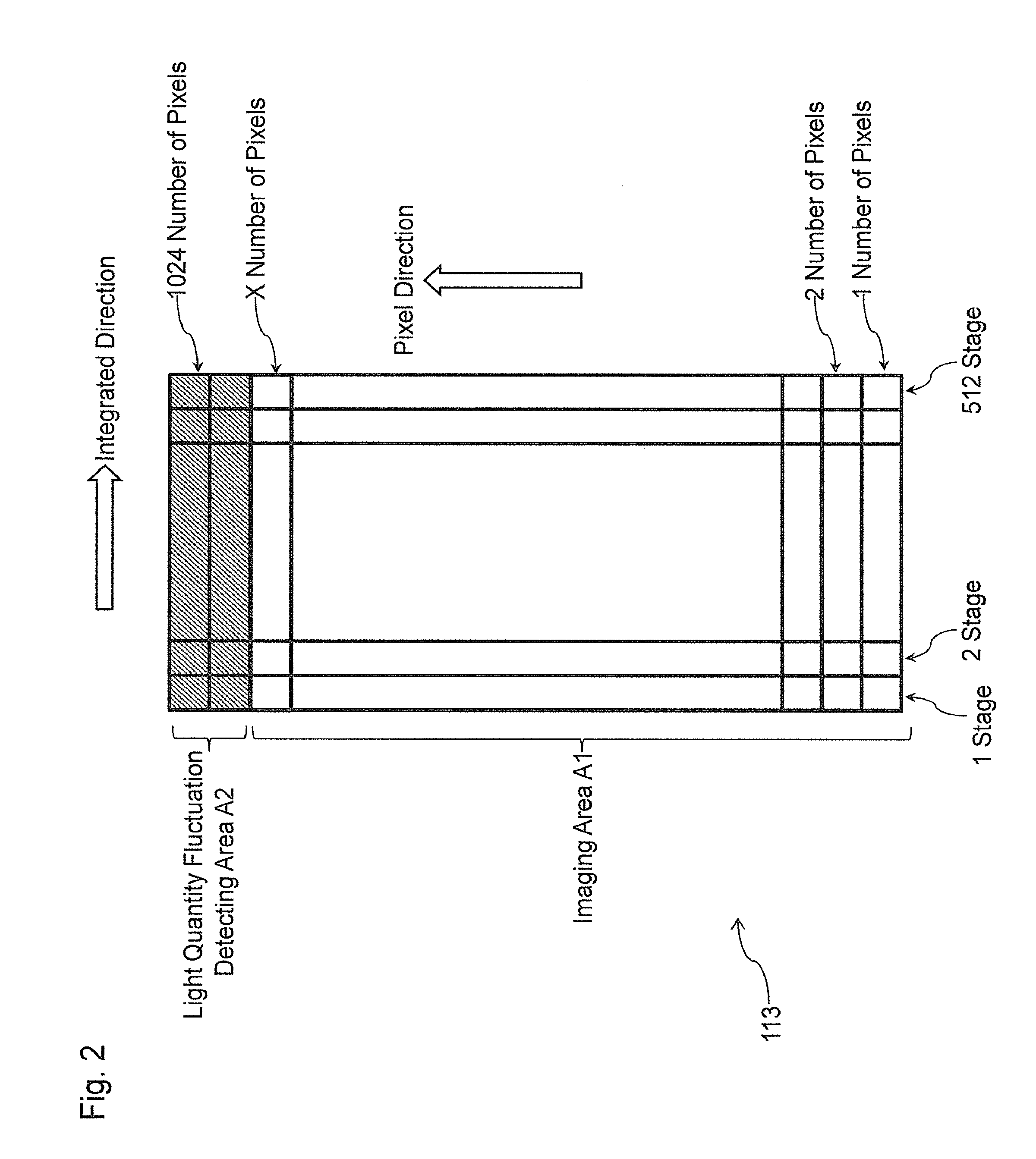
[0022]The components of the mask inspection apparatus 100, for acquiring optical data of the mask Ma, as one example of the object to be inspected, includes a table 101 that is movable in a horizontal direction (X-direction and / or Y-direction) and a rotation direction (θ-direction), a laser length measuring unit 102 that measures position coordinates of the ...


PUM

PropertyMeasurementUnit
lengthaaaaaaaaaa
widthaaaaaaaaaa
angleaaaaaaaaaa

Abstract

An inspection target is illuminated by an illumination optical unit using a light source. Optical image data of a pattern disposed in the inspection target is acquired by an imaging unit by causing light transmitted or reflected to be incident to a first and second area of a sensor. Reference image data is generated, corresponding to the optical image data, from design data of the pattern. The optical image data is corrected by obtaining a fluctuation of a gradation value of optical image data acquired using light incident to the second area, and correcting a gradation value of optical image data acquired using the light incident to the first area. A line width of the pattern of the corrected data, and a line width error which is a difference between the line widths of corrected data and reference image data are obtained by the line width error obtaining unit.

Description

CROSS-REFERENCE TO THE RELATED APPLICATION[0001]The entire disclosure of the Japanese Patent Application No. 2015-046478, filed on Mar. 9, 2015 including specification, claims, drawings, and summary, on which the Convention priority of the present application is based, are incorporated herein in its entirety.FIELD OF THE INVENTION[0002]The present invention relates to a Mask Inspection Apparatus and a Mask Inspection Method.BACKGROUND[0003]In a production process of a semiconductor element, an original pattern in which a circuit pattern is formed, that is, a mask or a reticle (hereinafter collectively referred to as a mask) is exposed and transferred onto a wafer by a reduction projection exposure apparatus called a stepper or a scanner. Since production of a Large Scale Integration (LSI) requires a large manufacturing cost, it is crucial to improve the production yield.[0004]A defect of a mask pattern can be cited as a large factor of degradation in the production yield of a semico...

Claims


Application Information

Patent Timeline
Patent Type & Authority Applications(United States)
IPC IPC(8): G06T7/00G01B11/00G01N21/956
CPCG06T7/0008G06T7/001G06T7/0018G01N21/95607G01N2201/06113G06T2207/30148G06T2207/10152G01N2021/95676G01N2201/12G01B11/002G06T5/50G06T2207/10056G06T5/92
Inventor YAMASHITAOGAWA, RIKI
Owner NUFLARE TECH INC
Learn More