Touch panel

a touch panel and display module technology, applied in the field of input devices, can solve the problems of increasing the number of components and the inability to reduce the thickness of the touch panel (or the display module), and achieve the effect of simple structure and easy incorporation into the electronic devi

Active Publication Date: 2016-09-29
SEMICON ENERGY LAB CO LTD
View PDF4 Cites 50 Cited by
  • Summary
  • Abstract
  • Description
  • Claims
  • Application Information

AI Technical Summary

Benefits of technology

[0018]Furthermore, it is required that an electronic device using a touch panel is reduced in thickness and weight. Therefore, a touch panel itself is required to be reduced in thickness and weight.
[0020]For example, in a touch panel (or a display module), a substrate provided with a touch sensor can be attached to the display surface side of a display panel. In other words, in a touch panel (or a display module), a display panel and a touch sensor can be separate components and can be attached to each other. However, in such a structure, a substrate for a touch sensor is needed in addition to a substrate for a display panel, resulting in that the thickness of a touch panel (or a display module) cannot be reduced and the number of components is increased.
[0021]An object of one embodiment of the present invention is to provide a thin touch panel (or a thin touch sensor equipped display device) and the like. Another object is to provide a touch panel (or a touch sensor equipped display device) with a simple structure and the like. Another object is to provide a touch panel (or a touch sensor equipped display device) which can be easily incorporated into an electronic device and the like. Another object is to provide a touch panel (or a touch sensor equipped display device) with a small number of components and the like. Another object is to provide a lightweight touch panel (or a lightweight touch sensor equipped display device) and the like.

Problems solved by technology

However, in such a structure, a substrate for a touch sensor is needed in addition to a substrate for a display panel, resulting in that the thickness of a touch panel (or a display module) cannot be reduced and the number of components is increased.

Method used


Image

  • Touch panel
  • Touch panel
  • Touch panel

Examples


embodiment 1

[0128]In this embodiment, a driving method, a mode, and a structure example of an input device or an input / output device of one embodiment of the present invention will be described with reference to the drawings.

[Example of Sensing Method of Sensor]

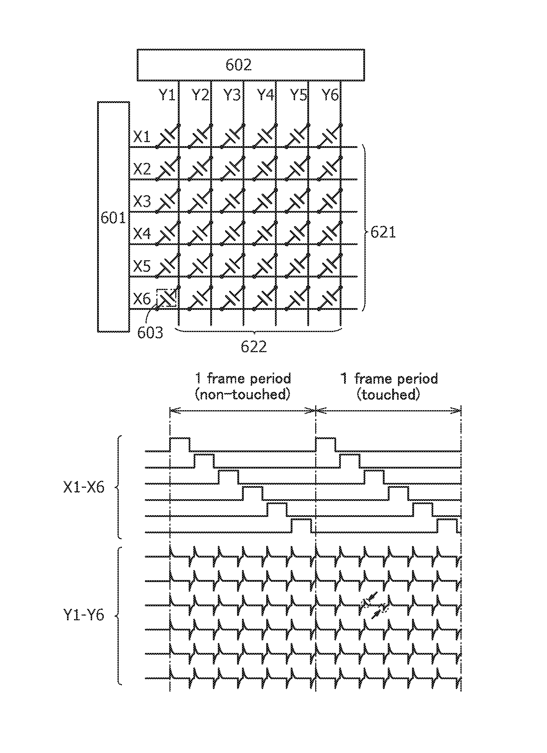
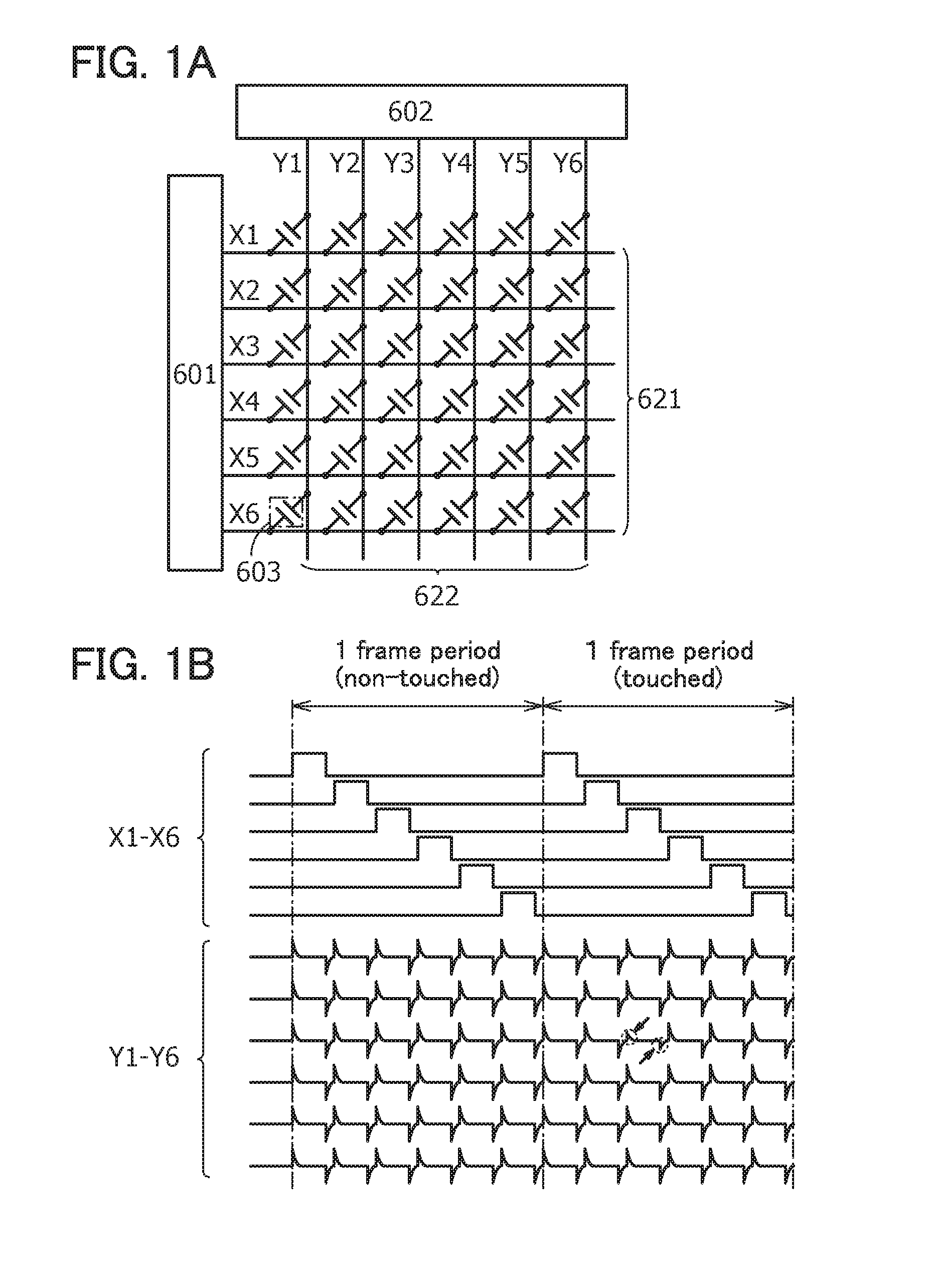
[0129]FIG. 1A is a block diagram illustrating the structure of a mutual capacitive touch sensor. FIG. 1A illustrates a pulse voltage output circuit 601 and a current sensing circuit 602. In FIG. 1A, as an example, six wirings X1 to X6 represent electrodes 621 to which a pulse voltage is applied, and six wirings Y1 to Y6 represent electrodes 622 that sense changes in current. The number of such electrodes is not limited to those illustrated in this example. FIG. 1A also illustrates a capacitor 603 that is formed with the electrodes 621 and 622 overlapping with each other or being provided very close to each other. Note that the functions of the electrodes 621 and 622 can be interchanged with each other.

[0130]The pulse voltage output circu...

structure example 1

[0203]More specific structure examples of the touch panel are described below.

[0204]FIG. 18A is a schematic perspective view of a touch panel 310 of one embodiment of the present invention. FIG. 18B is a schematic perspective developed view of FIG. 18A. Note that only main components are illustrated for simplicity. In FIG. 18B, some components (such as a substrate 372) are shown only in dashed outline.

[0205]The touch panel 310 includes a substrate 371 and the substrate 372 which are provided so as to face each other.

[0206]A display portion 381, a driver circuit 382, a wiring 383, a driver circuit 384, and the like are provided over the substrate 371. A conductive layer 332 is formed in the display portion 381. The substrate 371 is provided with an FPC 373 which is electrically connected to the wiring 383. In the example illustrated in FIGS. 18A and 18B, an IC 374 is provided over the FPC 373.

[0207]A surface of the substrate 372 which faces the substrate 371 is provided with a plural...

example 1

Cross-Sectional Structure Example 1

[0220]Examples of the cross-sectional structure of a touch panel of one embodiment of the present invention are described below with reference to the drawings.

Cross-Sectional Structure Example 1-1

[0221]FIG. 20 is a schematic cross-sectional view of the touch panel 310. FIG. 20 illustrates the cross sections of a region including the FPC 373, a region including the driver circuit 382, and a region including the display portion 381 in FIG. 18A.

[0222]The substrate 371 and the substrate 372 are attached to each other with an adhesive layer 151. A region surrounded by the substrate 371, the substrate 372, and the adhesive layer 151 is filled with liquid crystal 253.

[0223]A transistor 201, a transistor 203, a connection portion 206, a conductive layer 207, a conductive layer 251 and a conductive layer 252 included in a liquid crystal element 208, and the like are provided over the substrate 371.

[0224]An insulating layer 211, an insulating layer 212, an i...


PUM


Abstract

A touch panel which is thin, has a simple structure, or is easily incorporated into an electronic device is provided. The touch panel includes a first substrate, a second substrate, a first conductive layer, a second conductive layer, a third conductive layer, a fourth conductive layer, liquid crystal, and an FPC. The first conductive layer has a function of a pixel electrode. The second conductive layer has a function of a common electrode. The third and fourth conductive layers each have a function of an electrode of a touch sensor. The FPC is electrically connected to the fourth conductive layer. The first, second, third, and fourth conductive layers and the liquid crystal are provided between the first and second substrates. The first, second, and third conductive layers are provided over the first substrate. The FPC is provided over the first substrate.

Description

TECHNICAL FIELD[0001]One embodiment of the present invention relates to an input device. One embodiment of the present invention relates to a display device. One embodiment of the present invention relates to an input / output device. One embodiment of the present invention relates to a touch panel.[0002]Note that one embodiment of the present invention is not limited to the above technical field. One embodiment of the invention disclosed in this specification and the like relates to an object, a method, or a manufacturing method. One embodiment of the present invention relates to a process, a machine, manufacture, or a composition of matter. Specifically, examples of the technical field of one embodiment of the present invention disclosed in this specification and the like include a semiconductor device, a display device, a light-emitting device, a power storage device, a memory device, an electronic device, a lighting device, an input device, an input / output device, a driving method...

Claims


Application Information

Patent Timeline
Patent Type & Authority Applications(United States)
IPC IPC(8): G06F3/044
CPCG06F2203/04111G06F3/044G02F1/13338G06F3/0412G06F3/04166G06F3/0445G06F3/0446H10K59/40G06F3/041
Inventor KIMURA, HAJIMEYAMAZAKI, SHUNPEI
Owner SEMICON ENERGY LAB CO LTD
Why Eureka
Try Eureka