Organic light emitting diode display

Active Publication Date: 2016-09-29
SAMSUNG DISPLAY CO LTD
View PDF5 Cites 18 Cited by
  • Summary
  • Abstract
  • Description
  • Claims
  • Application Information

AI Technical Summary

Benefits of technology

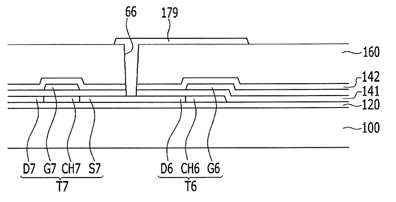
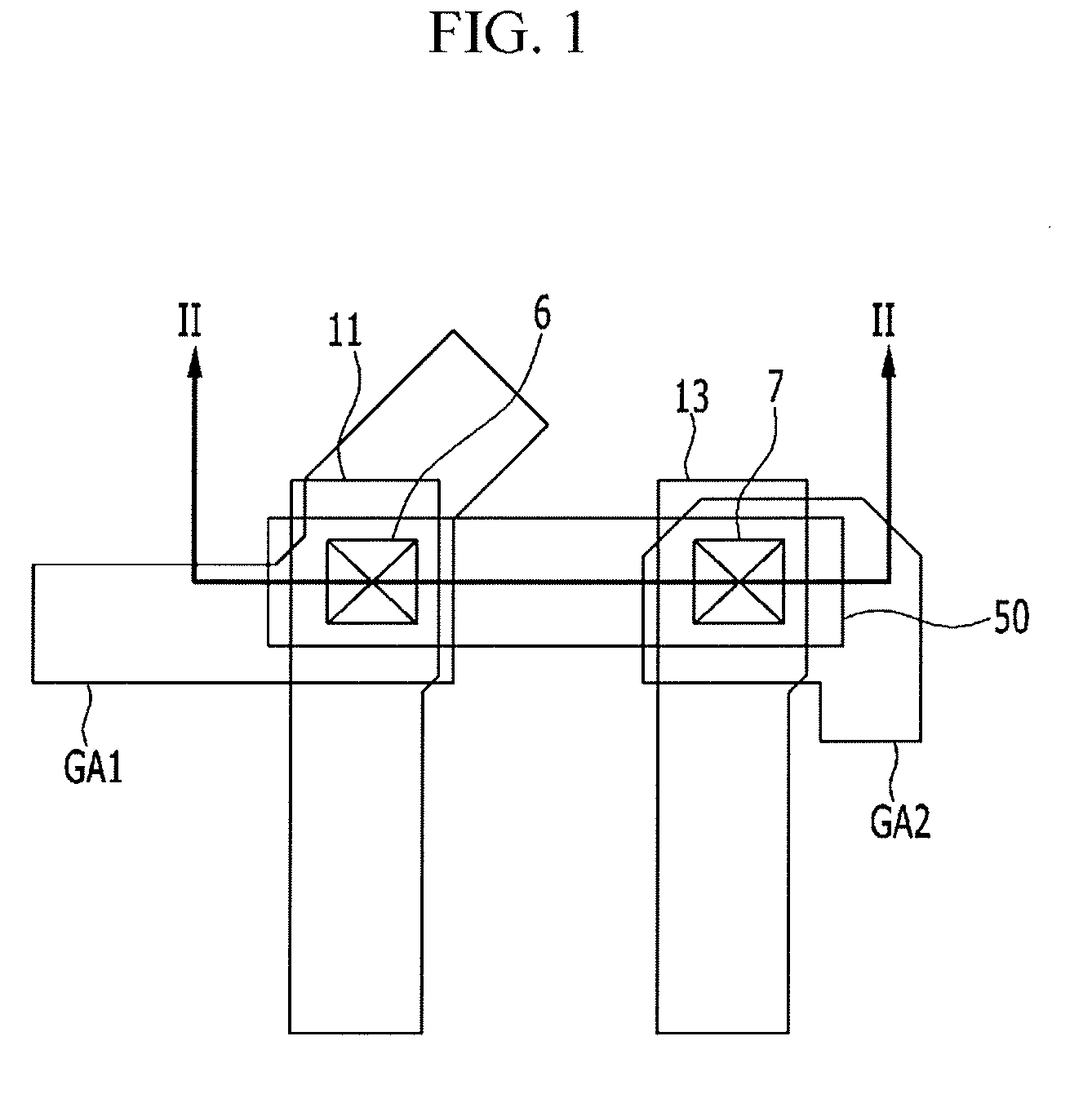
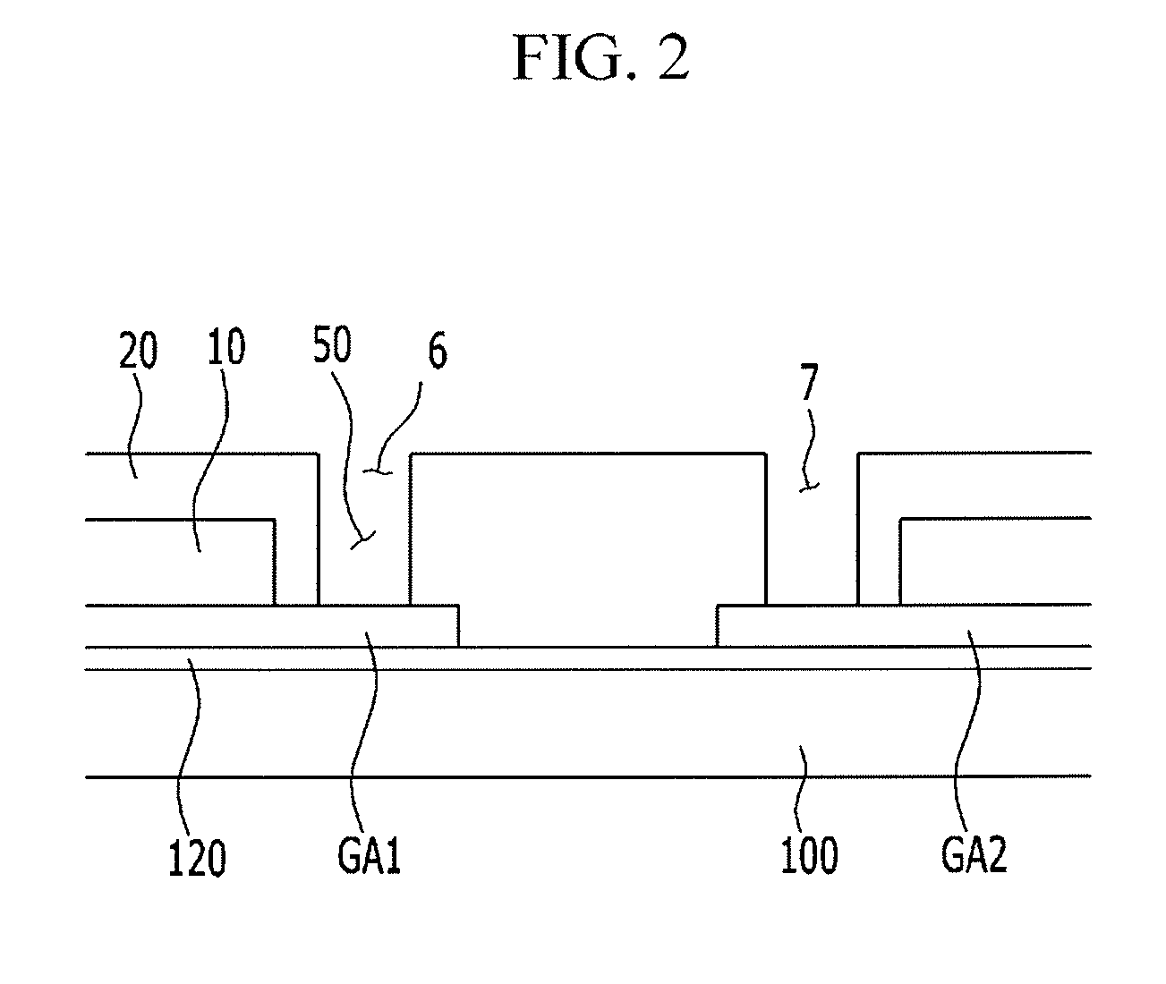
[0031]According to an exemplary embodiment of the present disclosure, parasitic capacitance can be minimized by positioning the organic layer between the signal lines on which crosstalk occurs.
[0032]Therefore, exemplary embodiments of the present disclosure can minimize crosstalk by minimizing the kickback voltage due to the parasitic capacitance to reduce the driving gate voltage Vg of the driving gate electrode connected to the first data connecting member, which is the driving gate node.
[0033]Further, exemplary embodiment of the present disc

Problems solved by technology

However, changes in the voltage of a data line or the scan signal of a scan line can affect a voltage of a driving gate node of the driving transistor due to a parasitic capacitance formed between the driving gate node connected to a driving gate electrode of the driving transistor and the data line, or a parasitic capacitance at a portion where the driving gate node of the driving transistor overlaps the scan line.
The change in voltage of the driving gate node changes a driving current flowi

Method used


Image

  • Organic light emitting diode display
  • Organic light emitting diode display
  • Organic light emitting diode display

Examples


Example

[0055]Embodiments of the present disclosure will be described more fully hereinafter with reference to the accompanying drawings, in which exemplary embodiments of the disclosure are shown. As those skilled in the art would realize, the described embodiments may be modified in various different ways, all without departing from the spirit or scope of the present disclosure.

[0056]Accordingly, the drawings and description are to be regarded as illustrative in nature and not restrictive. Like reference numerals may designate like elements throughout the specification.

[0057]In the drawings, the thickness of layers, regions, etc., may be exaggerated for clarity.

[0058]Further, throughout the present specification, it will be understood that when an element such as a layer, film, region, or substrate is referred to as being “on” another element, it can be directly on the other element or intervening elements may also be present.

[0059]Further, an active matrix (AM) type organic light emittin...


PUM


Abstract

An organic light emitting diode display includes a substrate, a semiconductor disposed on the substrate that includes a channel for each of a plurality of transistors and doping regions formed at both sides of each channel; a gate insulating layer disposed on the semiconductor that includes an insulating layer opening through which the doping regions of two different transistors are exposed; a gate electrode disposed on the gate insulating layer that overlaps each channel; an interlayer insulating layer disposed on the gate electrode that includes a first and second contact holes through which the doping regions exposed within the insulating layer opening are each exposed; and data wirings disposed on the interlayer insulating layer that are each connected to the doping regions. The interlayer insulating layer includes an organic layer, and the first and second contact holes each include a first side wall positioned within the insulating layer opening.

Description

CROSS-REFERENCE TO RELATED APPLICATION[0001]This application claims priority under 35 U.S.C. §119 from, and the benefit of, Korean Patent Application No. 10-2015-0045236, filed in the Korean Intellectual Property Office on Mar. 26, 2015, the contents of which are herein incorporated by reference in their entirety.BACKGROUND[0002]1. Technical Field[0003]Embodiments of the present disclosure are directed to an organic light emitting diode display.[0004]2. Discussion of the Related Art[0005]An organic light emitting diode display includes two electrodes and an organic emission layer disposed therebetween and forms excitons by combining electrons injected from one electrode with holes injected from another electrode at the organic emission layer, and emits light by allowing the excitons to emit energy.[0006]An organic light emitting diode display includes a plurality of pixels, each including an organic light emitting diode, which is a self-light emitting device, and each provided with ...

Claims


Application Information

Patent Timeline
IPC IPC(8): H01L27/32
CPCH01L27/3276H01L27/3246H01L27/3258H01L27/3262H01L27/1255H01L27/3248H01L27/1248H01L27/124H01L27/3265H01L27/1225H10K59/123H10K59/124H10K59/131H10K59/1201G09G3/3208H10K59/10H10K59/122H10K59/125H10K59/1213H10K59/1216
Inventor LEE, WANG WOOPARK, YOUNG WOOSON, SE WANWOO, MIN WOO
Owner SAMSUNG DISPLAY CO LTD
Why Eureka
Try Eureka