Symmetrical extension junction formation with low-k spacer and dual epitaxial process in finfet device

a technology of low-k spacer and extension junction, which is applied in the direction of semiconductor devices, basic electric elements, electrical equipment, etc., can solve the problem of difficult to completely turn off the transistor

Inactive Publication Date: 2016-09-29
IBM CORP
View PDF0 Cites 15 Cited by
  • Summary
  • Abstract
  • Description
  • Claims
  • Application Information

AI Technical Summary

Problems solved by technology

With advanced geometry planar FET technologies, such as 20 nanometer (nm) fabrication, the source and the drain encroach into the channel, making it easier for leakage current to flow between them and in turn making it very difficult to turn the transistor off completely.

Method used


Image

  • Symmetrical extension junction formation with low-k spacer and dual epitaxial process in finfet device
  • Symmetrical extension junction formation with low-k spacer and dual epitaxial process in finfet device
  • Symmetrical extension junction formation with low-k spacer and dual epitaxial process in finfet device

Examples


Embodiment Construction

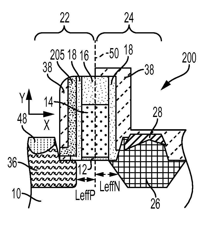
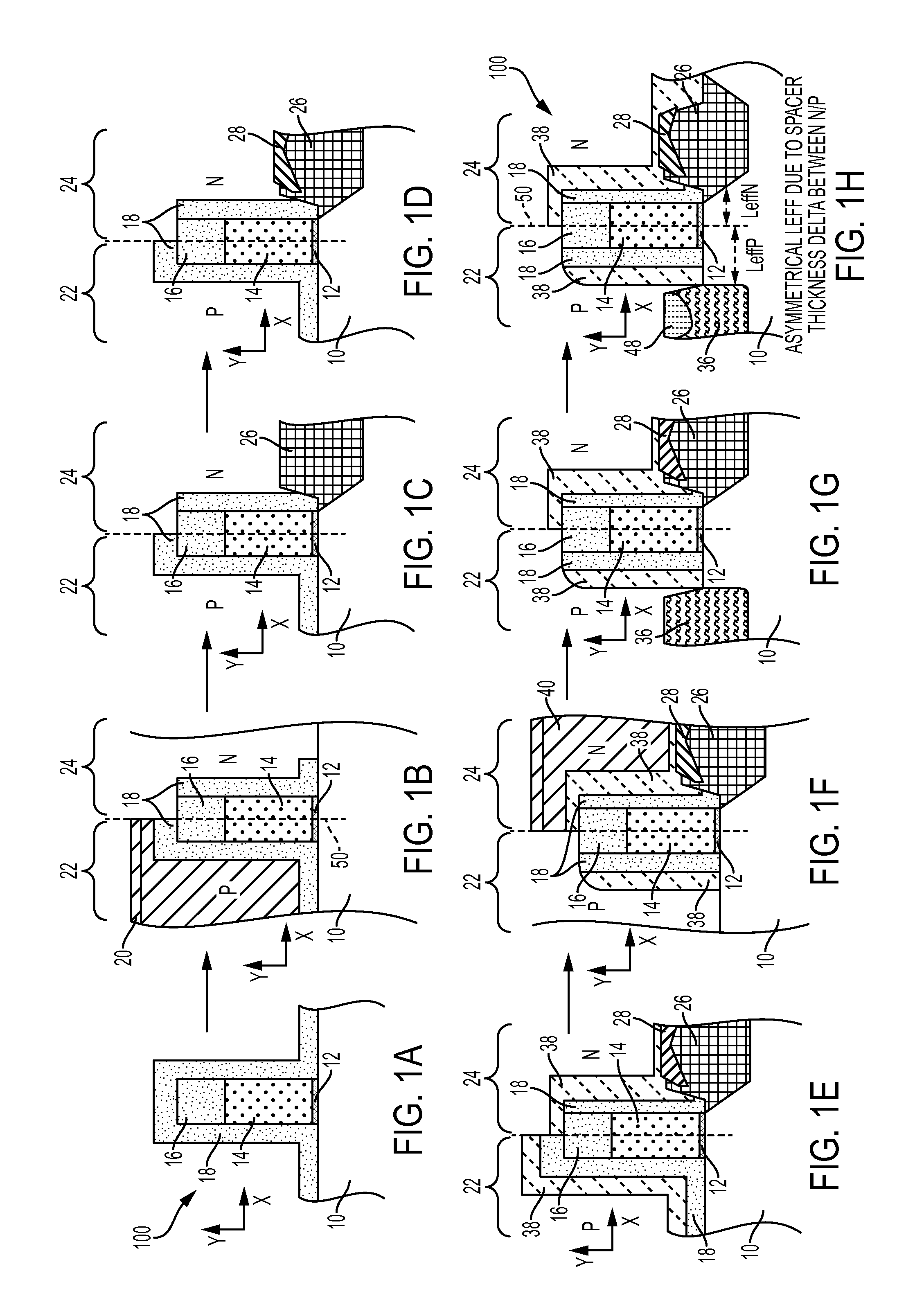
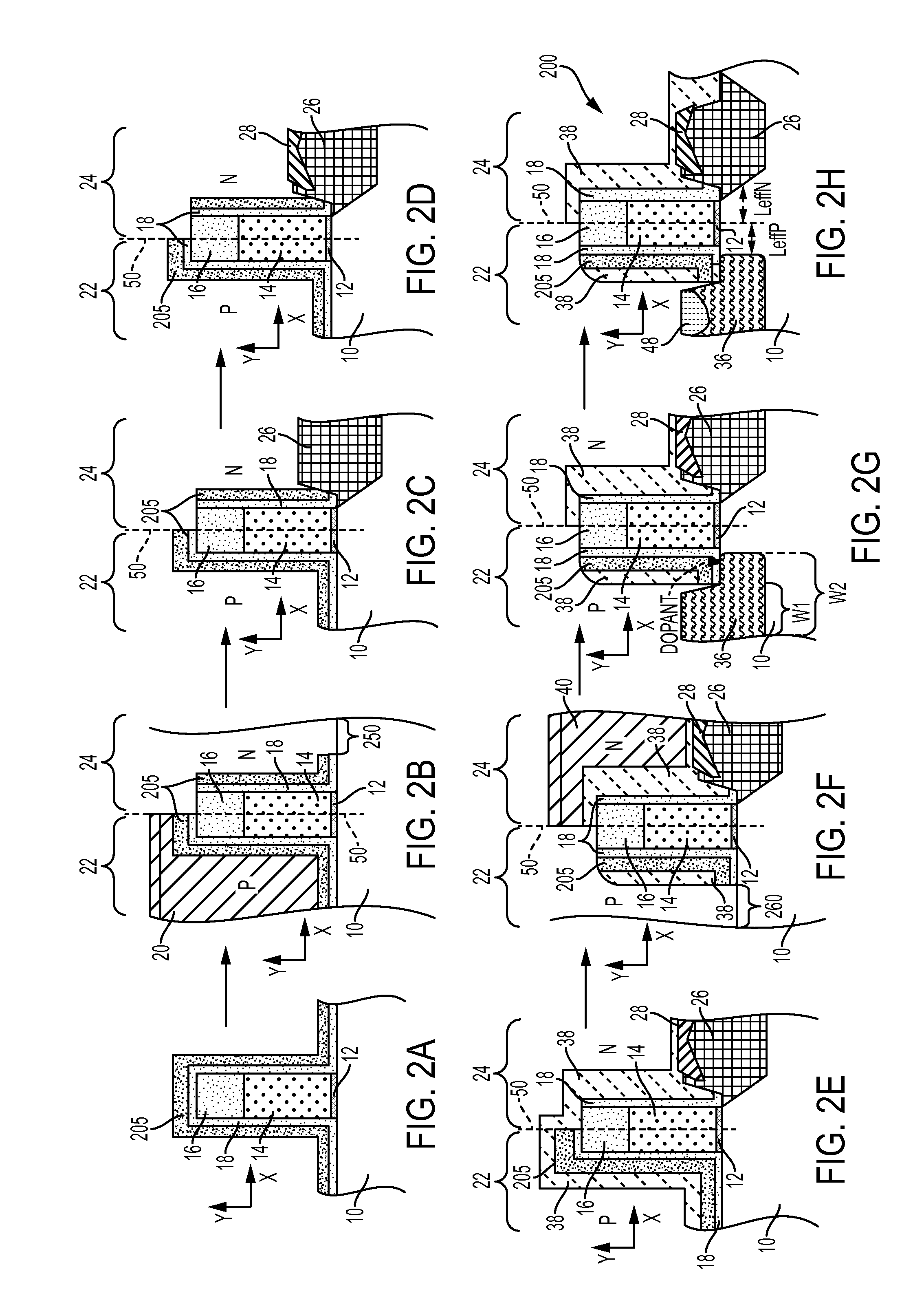
[0028]Dual spacer and dual epitaxial layers (epi) for n-type (n-channel) field effect transistors (NFET) and p-type (p-channel) field effect transistors (PFET) are utilized to optimize the junction between the n-type and p-type (such as the source / drain) regions, thereby growing the fins (i.e., epitaxial layers) of the finFET device.

[0029]FinFET technology features a dual epitaxial layer process for damage-less conformal diffusion during extension junction formation. One issue with the dual epitaxial layer process is epitaxial overburden which causes parasitic capacitance. Embodiments utilize a low-k spacer to address the epitaxial overburden that causes parasitic capacitance in the dual epitaxial layer process.

[0030]Another issue in the dual epitaxial layer process is the introduction of block nitride (e.g., 3 nm). The purpose of the block nitride is to block the epitaxial layer formation from either side as its name suggests, such that each epitaxial layer remains on its own side....


PUM


Abstract

A technique relates to a dual epitaxial process a device. A first spacer is disposed on a substrate, dummy gate, and hardmask. A first area extends in a first direction from the gate and a second area extends in an opposite direction. A doped intermediate spacer is disposed on the first spacer. A first region is opened on the substrate by removing first spacer and intermediate spacer at the first region. A first epitaxial layer is disposed in the first region. The intermediate spacer is removed from first area. A second spacer is disposed on the intermediate spacer. A second region is opened on the substrate by removing the first spacer, intermediate spacer, and second spacer. A second epitaxial layer is disposed in second region. The width of the second epitaxial layer is enlarged by annealing causing dopant in the intermediate spacer layer to flow into the second epitaxial layer.

Description

[0001]This application is a continuation of U.S. patent application Ser. No. 14 / 671,115, filed Mar. 27, 2015, the disclosure of which is incorporated by reference herein in its entirety.BACKGROUND[0002]The present invention relates to semiconductor device manufacturing techniques, and more specifically, to the symmetrical extension junction formation with a low-k spacer and dual epitaxial process in finFET devices.[0003]While the planar field effect transistor (FET) may appear to have reached the end of its scalable lifespan, the semiconductor industry has found an alternative approach with finFETs. FinFET technology is viewed by many as the best choice for next generation advanced processes.[0004]With advanced geometry planar FET technologies, such as 20 nanometer (nm) fabrication, the source and the drain encroach into the channel, making it easier for leakage current to flow between them and in turn making it very difficult to turn the transistor off completely. FinFETs are three...

Claims


Application Information

Patent Timeline
Patent Type & Authority Applications(United States)
IPC IPC(8): H01L29/66H01L21/324
CPCH01L29/66795H01L21/324H01L29/66545H01L29/66553
Inventor BASKER, VEERARAGHAVAN S.LIU, ZUOGUANGYAMASHITA, TENKOYEH, CHUN-CHEN
Owner IBM CORP
Why Eureka
Try Eureka