Check patentability & draft patents in minutes with Patsnap Eureka AI!

Nonvolatile memory interface for metadata shadowing

Active Publication Date: 2016-10-06
IBM CORP
View PDF3 Cites 3 Cited by
  • Summary
  • Abstract
  • Description
  • Claims
  • Application Information

AI Technical Summary

Benefits of technology

This patent is about a way to manage memory on a device by streaming data to the device's memory buffer using a high-speed write data channel. The method uses special assets to optimize the speed of writing to the device's memory cells. On the other hand, the method also allows for reading data from the device using a read channel that includes no design requirements for high-speed or low-latency data transmission. The main technical effect of the patent is to improve the speed and efficiency of writing and reading data to and from memory devices.

Problems solved by technology

However, there are potential applications for nonvolatile memory devices that are limited by the use of SRAM- or DRAM-type interfaces.
Memory interfaces for symmetric operations are generally designed for generic applications, leading to a cost increase in low-margin, high volume applications such as hard drives and SSDs.

Method used


Image

  • Nonvolatile memory interface for metadata shadowing
  • Nonvolatile memory interface for metadata shadowing
  • Nonvolatile memory interface for metadata shadowing

Examples


Embodiment Construction

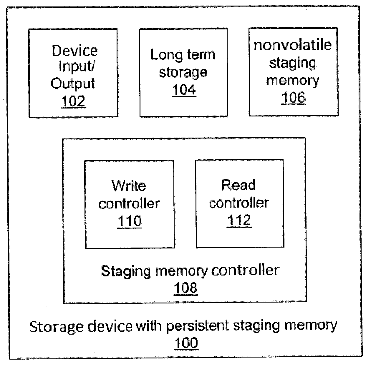
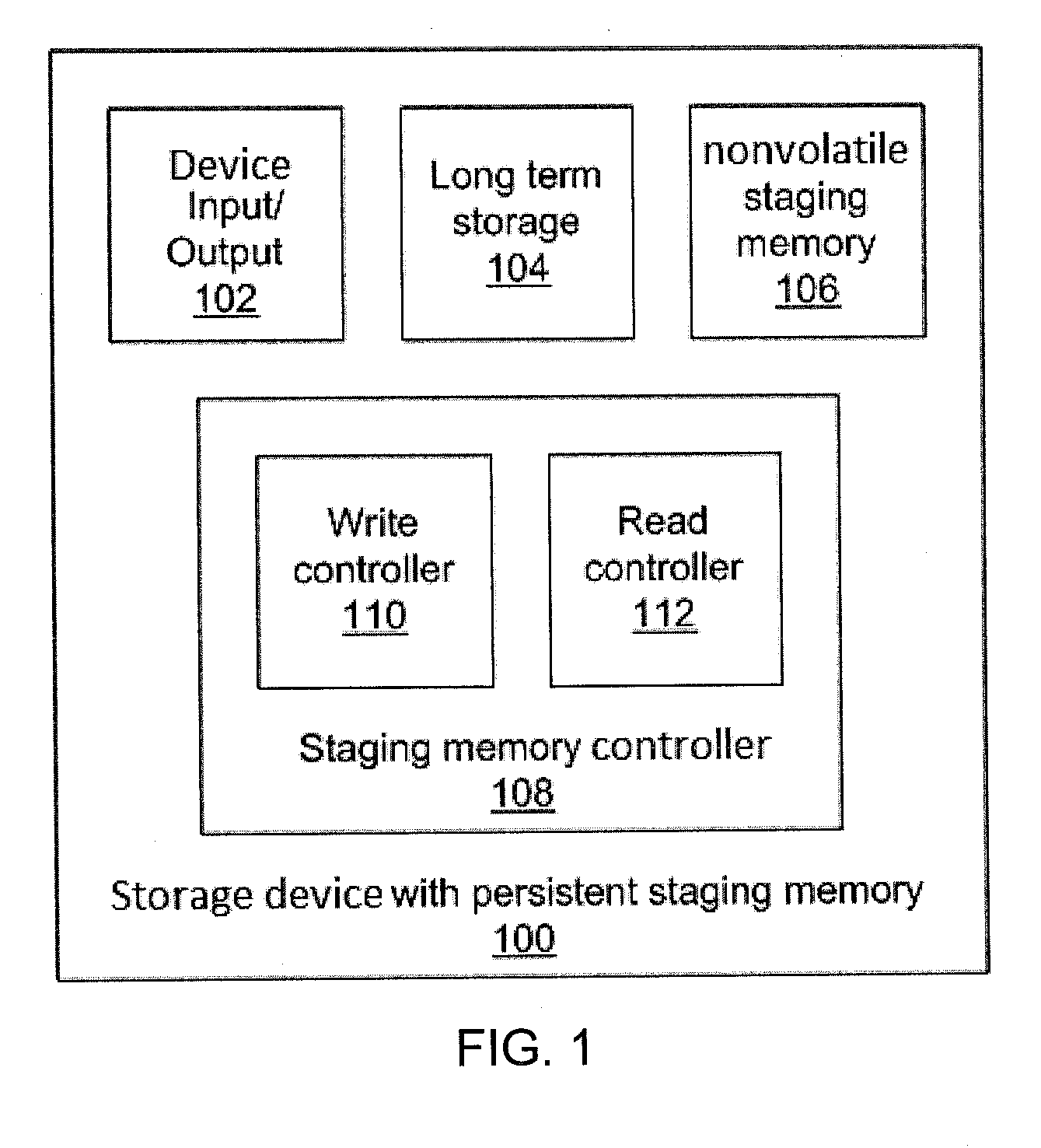
[0022]Embodiments of the present principles provide an interface to nonvolatile memory, including magnetoresistive random access memory (MRAM), that is particularly well suited to use in a persistent staging buffer for metadata (and potentially also data) for storage devices, including hard disk drives (HDDs) and solid state drives (SSDs). The present embodiments thereby contribute to the construction of a fully persistent (or at least robustly consistent, in the case of metadata-only staging) storage device without the use of any backup power. By omitting batteries, capacitors, and the like, the size and cost of the devices may be reduced.

[0023]Metadata is used in storage to express the structure, both spatial and temporal, of the storage device and the stored data. Such data needs to be consistent, maintaining a valid and representative state of the memory at all times. Changes in the metadata track changes in the data and data structure, and a loss of metadata not only means a lo...


PUM


Abstract

A memory includes non-volatile memory devices, each of which has multiple nonvolatile memory cells. A write controller streams bits to the memory devices in groups of N bits using a write data channel having write bus drivers, receivers and write bus topology that take advantage of high-speed signaling to optimize a speed of writing to the memory devices. Consecutive groups of bits are written to consecutive memory cells within respective memory devices. A self-referenced read controller reads bits from the memory devices using a read channel having read drivers, receivers, and read bus topology that include no design requirements for high-speed or low-latency data transmission.

Description

BACKGROUND[0001]1. Technical Field[0002]The present invention relates to nonvolatile memory, including magnetoresistive random access memory. More particularly the present invention relates to a new type of interface for such nonvolatile memory.[0003]2. Description of the Related Art[0004]Most existing magnetoresistive random access memory (MRAM) offerings include very low-density chips with a static RAM (SRAM) interface. Present research for MRAM packaging is geared toward improving density with the aim of making MRAM a candidate for replacing dynamic RAM (DRAM). Phase Change Memory (PCM) is another type of nonvolatile memory. DRAM interfaces are appearing on both MRAM and PCM chips. However, there are potential applications for nonvolatile memory devices that are limited by the use of SRAM- or DRAM-type interfaces. Some MRAM interfaces are multibit, symmetric serial interfaces. To date, all of these SRAM-type, DRAM-type, and serial interfaces are symmetric interfaces, with equal o...

Claims


Application Information

Patent Timeline
IPC IPC(8): G11C11/16
CPCG11C11/1673G11C11/1675G11C7/1015G11C13/0004G11C13/004G11C13/0061G11C13/0069G11C11/1693G11C7/10G11C7/1003G06F13/1668G06F3/0602G06F3/0659G06F3/0673G06F3/061G06F3/0688G06F3/0613G06F3/0656G06F3/0679
Inventor DEBROSSE, JOHN K.FITCH, BLAKE G.FRANCESCHINI, MICHELE M.TAKKEN, TODD E.WORLEDGE, DANIEL C.
Owner IBM CORP
Features
  • R&D
  • Intellectual Property
  • Life Sciences
  • Materials
  • Tech Scout
  • Unparalleled Data Quality
  • Higher Quality Content
  • 60% Fewer Hallucinations
Learn More