Method of designing semiconductor integrated circuit device and semiconductor integrated circuit device

a technology of integrated circuits and semiconductors, applied in the direction of solid-state devices, semiconductor/solid-state device details, instruments, etc., can solve the problems of increased design effort, increased design inconvenience, and increased design cost, so as to reduce design and labor burden, chip size, power consumption and operating speed are optimized, and the effect of reducing the burden on design and labor

Inactive Publication Date: 2005-12-22
RENESAS ELECTRONICS CORP
View PDF19 Cites 38 Cited by
  • Summary
  • Abstract
  • Description
  • Claims
  • Application Information

AI Technical Summary

Benefits of technology

[0008] An object of the present invention is to provide a design technique capable of implementing ICs which are different in cell type from each other without having to increase the burden on the designer.
[0009] Another object of the present invention is to provide a design technique capable of easily implementing a semiconductor integrated circuit device in which its chip size, power consumption and operating speed are optimized.
[0014] According to the above feature, since only one kind of cell may be designed for circuits having the same function, a maker can reduce the burden on the design and labor, such as the extraction of characteristics such as voltage dependency, temperature dependency, delay times or the like of each designed cell, the description thereof in the specifications, etc., and, in its turn, achieve a reduction in cost as well.
[0015] Further, a semiconductor integrated circuit device wherein the chip size, power consumption and operating speed are optimized, can easily be implemented by properly using substrate potential fixed and variable cells according to the functions or the like of circuit portions used with cells on one semiconductor chip and mixing them together in this condition.

Problems solved by technology

As a result, it became evident that the following problems were inherent in such a device.
When the threshold of each MOSFET is controlled using the above described substrate bias effect in an attempt to realize an IC having desired characteristics, an inconvenience occurs in that wiring or wires for supplying the bias voltages to the well regions used as the bases of the respective MOSFETs are required in large numbers (Vcc line, Vbp / Ncc line, Vss line and Vbn / Nss line) and the area occupied by the circuit, and, in turn, the chip size of the IC, increases.
Therefore, the design effort increases, and the labor, such as the extraction of characteristics including delay times or the like of the circuit cells, required when the user designs and evaluates the chip using these circuit cells, the description thereof in the specifications (data sheet or data book), etc. also increases, i.e., the burden of preparing respective specifications for corresponding cell libraries increases.

Method used


Image

  • Method of designing semiconductor integrated circuit device and semiconductor integrated circuit device
  • Method of designing semiconductor integrated circuit device and semiconductor integrated circuit device
  • Method of designing semiconductor integrated circuit device and semiconductor integrated circuit device

Examples


Embodiment Construction

[0055] Preferred embodiments of the present invention will hereinafter be described with reference to the accompanying drawings.

[0056] A description will first be made of how to view common cell topology, using a CMOS (Complementary MOS) inverter cell INV as an illustrative example.

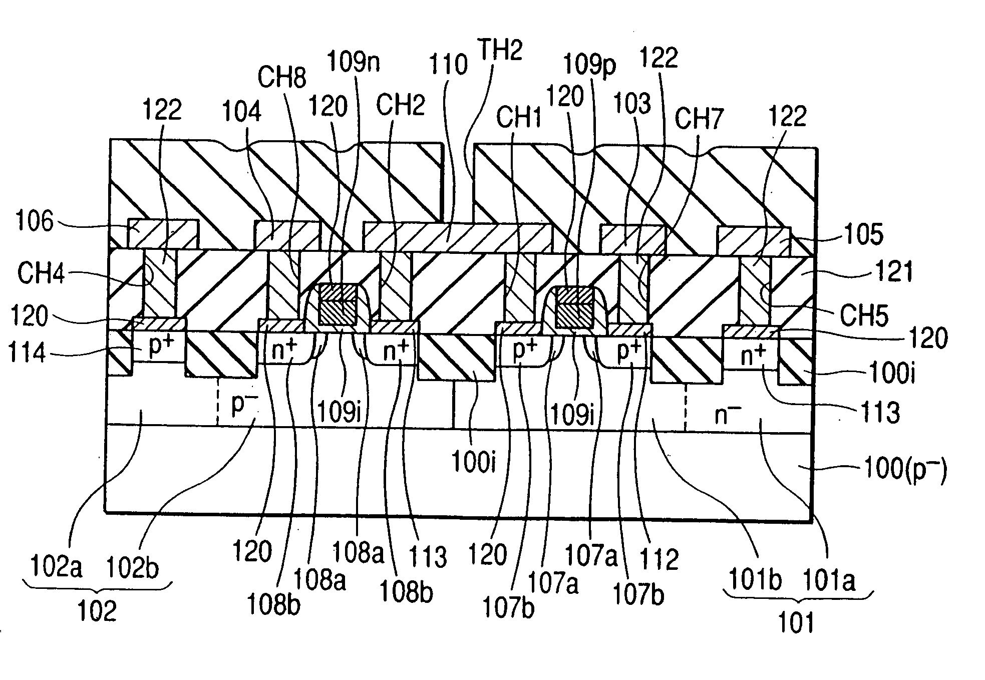
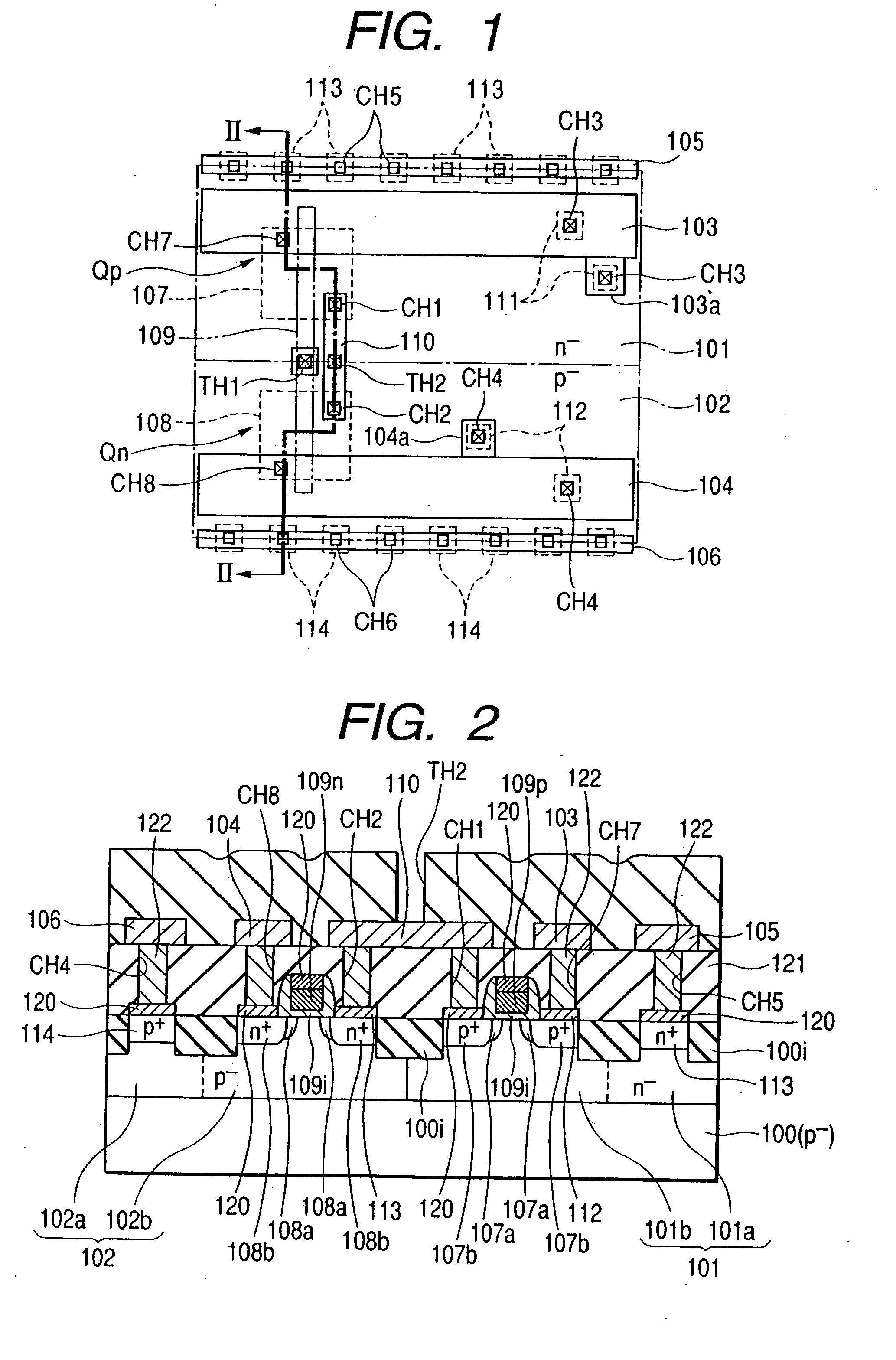
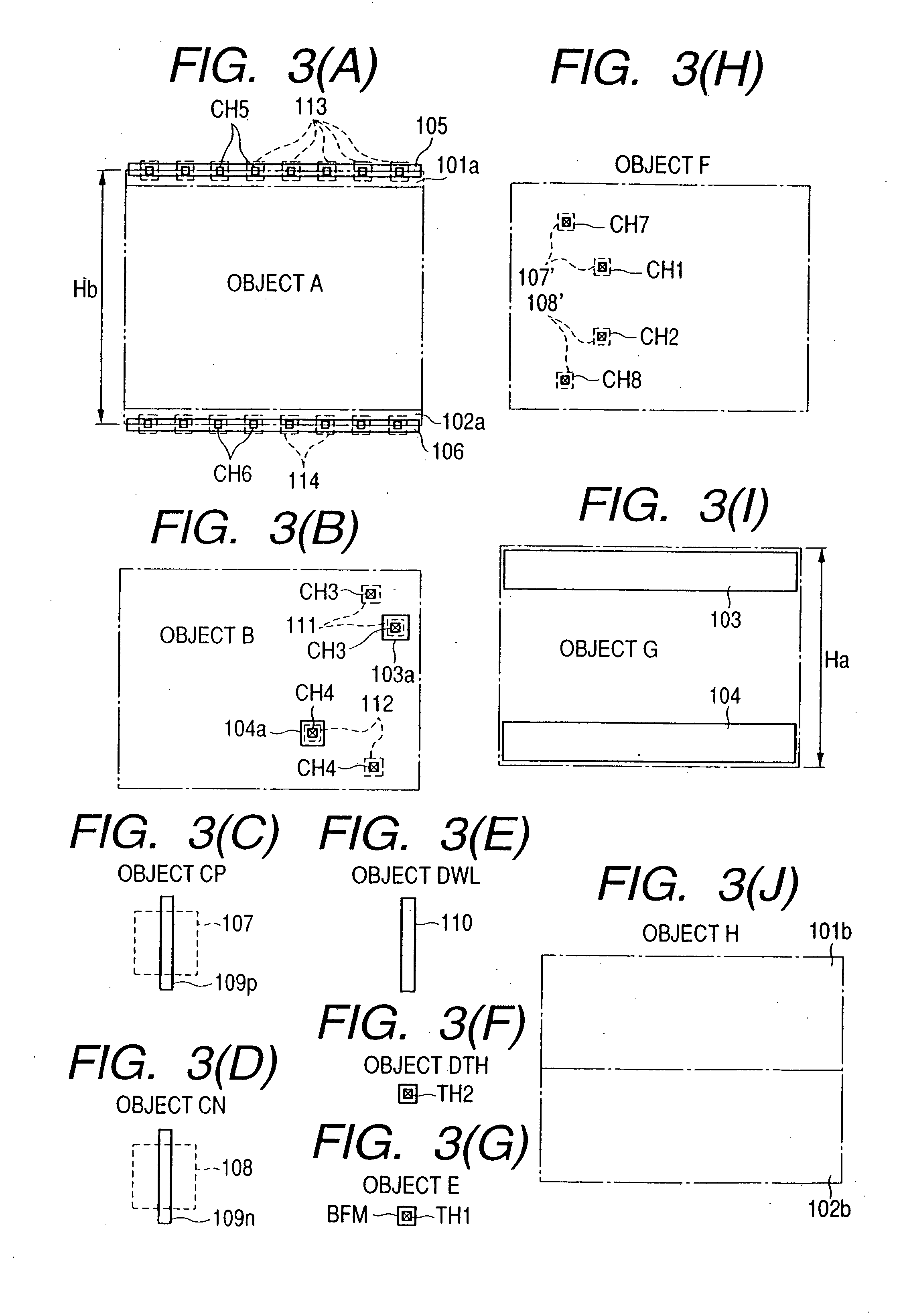
[0057]FIGS. 1 and 2 respectively show one example of a common cell topology for a CMOS inverter cell INV comprised of a pair of elements including a p channel MISFET (Metal Insulator Semiconductor FET) Qp and an n channel MISFET Qn. Of these, FIG. 1 illustrates an example of a layout pattern of a circuit cell and FIG. 2 shows an example of a sectional view taken along line 11 - II of FIG. 1.

[0058] In FIGS. 1 and 2, reference numeral 100 indicates a p-type single-crystal silicon substrate used as a base, for example. Reference numeral 100i indicates a device or element separator, and reference numerals 101 and 102 indicate an n well region (101a, 101b) and a p well region (102a, 102b) defined as relativ...


PUM


Abstract

In a semiconductor integrated circuit device and a method of designing the same, design information about circuit cells each having a desired function are described as objects according to selected purposes. The pieces of design information are registered in a cell library as cell information capable of forming any of substrate potential fixed cells and substrate potential variable cells. Further, a data sheet common to the substrate potential fixed cell and the substrate potential variable cell is offered to a user, so that the user is able to make a selection according to the user's purposes. The substrate potential fixed cells and the substrate potential variable cells are mixed together on a semiconductor chip so as to be properly used according to the functions or the like of circuit portions in which the cells are used.

Description

[0001] This application is a continuation of U.S. application Ser. No. 10 / 440,162, filed May 19, 2003, which, in turn, is a continuation of U.S. application Ser. No. 09 / 939,699, filed Aug. 28, 2001 (now U.S. Pat. No. 6,611,943), and which, in turn, is a divisional of U.S. application Ser. No. 09 / 131,393, filed Aug. 7, 1998 (now U.S. Pat. No. 6,340,825); and the entire disclosures of all of which are hereby incorporated by reference.[0002] This invention relates to a method of designing a semiconductor integrated circuit device, and a technique effective in a case in which a plurality of circuits different in characteristic from each other are prepared as a cell library and a user selects a desired circuit from the cell library in the course of design of a semiconductor integrated circuit device. This invention also relates to a technique which is effective for use in the design of an ASIC (Application Specific Integrated Circuit), for example. [0003] It has been known that a semicon...

Claims


Application Information

Patent Timeline
Patent Type & Authority Applications(United States)
IPC IPC(8): H01L21/822G06F17/50G11C8/00H01L21/336H01L21/82H01L27/00H01L27/02H01L27/04H01L27/118H01L29/78
CPCH01L27/0207H01L27/11807H01L2924/0002H01L2924/00H01L25/18
Inventor SHIBATA, RYUJISHIMADA, SHIGERU
Owner RENESAS ELECTRONICS CORP
Why Eureka
Try Eureka