Method for removing photoresist as well as method for reworking of photoetching technology

A technology of photoresist and photoresist layer, which is applied in the direction of photosensitive material processing, electrical components, semiconductor/solid-state device manufacturing, etc., can solve the problem of residual photoresist that cannot be removed from the surface of semiconductor wafers, etc., to achieve extended The effect of process time

Inactive Publication Date: 2008-10-08
SEMICON MFG INT (SHANGHAI) CORP
View PDF1 Cites 39 Cited by
  • Summary
  • Abstract
  • Description
  • Claims
  • Application Information

AI Technical Summary

Problems solved by technology

[0010] Therefore, the present invention provides a method for removing photoresist and a rework method of photolithography process, so as to solve the problem that existing methods cannot completely remove photoresist residues on the surface of semiconductor wafers and have residual defects

Method used


Image

  • Method for removing photoresist as well as method for reworking of photoetching technology
  • Method for removing photoresist as well as method for reworking of photoetching technology

Examples


Embodiment Construction

[0034] The specific embodiments of the present invention will be described in detail below in conjunction with the accompanying drawings.

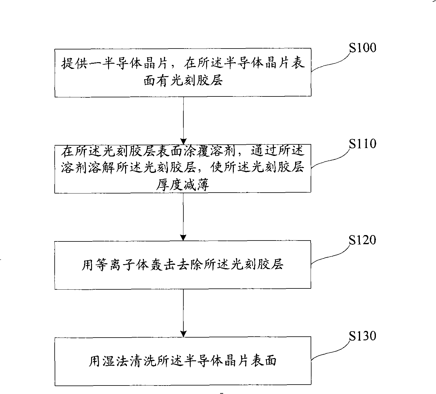
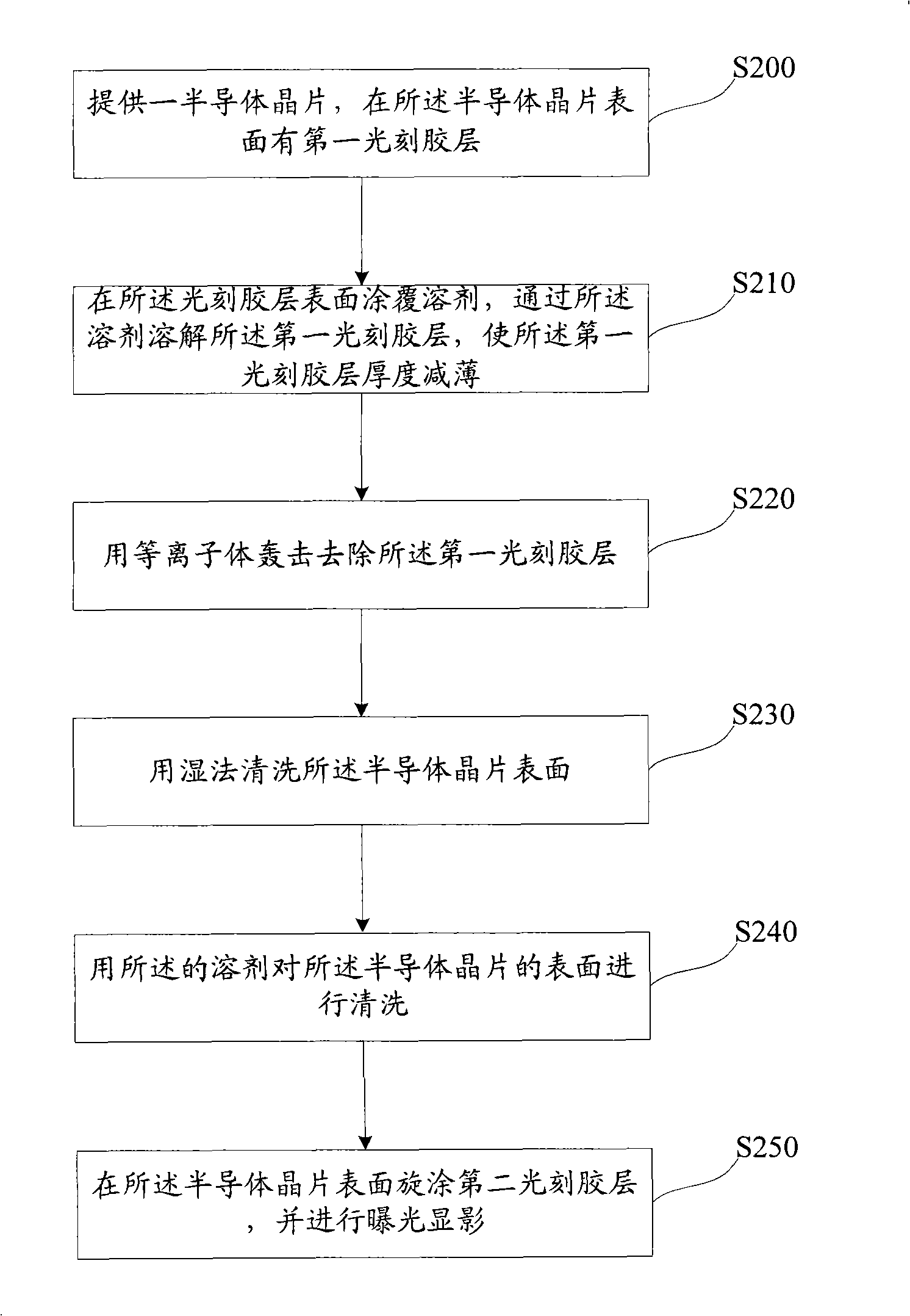
[0035] figure 1 It is a flowchart of an embodiment of the photoresist removal method of the present invention.

[0036] Such as figure 1As shown, in step 1, a semiconductor wafer is provided, and there is a photoresist layer on the surface of the semiconductor wafer (S100). The material of the semiconductor wafer may be one of single crystal silicon, polycrystalline silicon, amorphous silicon, gallium arsenide, and silicon germanium compound, and the semiconductor wafer may also include a silicon-on-insulator structure. The photoresist layer can be a photoresist layer to be removed after etching or ion implantation; it can also be a photoresist layer with a pattern after the photolithography process is completed. Finally, inspect the photoresist layer that needs to be removed with defect residues, or the photoresist layer that needs to ...


PUM


Abstract

A method of removing photosensitive resist comprises providing a semiconductor chip with photosensitive resist layer at surface; the solvent is coated at the surface of the photosensitive resist layer; the photosensitive resist layer is solved by the solvent so as to thicken the thickness of the photosensitive resist layer; the photosensitive resist layer is removing by bombarding by plasma; the semiconductor surface is cleaned by wet method. The method is used in the reworking method of photoetching technology. The method in the invention is able to cleanly remove the photosensitive resist on the surface of the semiconductor chip, and does not damage the surface of the semiconductor chip.

Description

technical field [0001] The invention relates to the technical field of semiconductor manufacturing, in particular to a photoresist removal method and a photolithographic rework method. Background technique [0002] Photolithography plays a pivotal role in the semiconductor manufacturing process. In the semiconductor manufacturing process, it is necessary to pre-define a photoresist pattern on the semiconductor substrate by photolithography, and then perform etching or ion implantation according to the predetermined pattern. The level and quality of photolithography process directly affect the results of etching or ion implantation. In photolithography, the photoresist is first uniformly spin-coated on the surface of the semiconductor wafer by spin coating, and then the pattern on the mask plate is transferred to the surface of the semiconductor wafer through a series of processes such as baking, exposure, and development. Form a pattern on the photoresist. Its main steps ...

Claims


Application Information

Patent Timeline
Patent Type & Authority Applications(China)
IPC IPC(8): G03F7/42G03F7/36H01L21/027
Inventor 杨光宇
Owner SEMICON MFG INT (SHANGHAI) CORP
Why Eureka
Try Eureka