However, as saw manufacturers have struggled to meet this demand for wafer cutting saws that can
cut thinner and thinner wafers, they have been met with complaints of broken wafers, wafer thickness variations, wafer
surface roughness, etc.
In addition, the use of
silicon carbide, a known
carcinogen, as a
cutting agent along with
ethylene glycol as the cutting medium, presents additional environmental hazards which must be dealt with, and recycling of materials and fluids involved in such operations is expensive.
Among other things, this results in broken wafers, chips, and some wafers being thicker while others are thinner, a problem known as the “thick-thin” problem.
As can be imagined, this is a slow process for cutting, and the consistency of the slurry mixture has to be well controlled to avoid
waviness, inconsistent thickness,
scratching or other quality problems in the cut wafers.
However, the use of viscous cleansing fluid, i.e.
ethylene glycol, remains an
environmental hazard problem, a quality problem in the cut wafers, and also a cost problem for the user.
However, water has some drawbacks.
First, water inherently has an abundance of
oxygen in it.
This
surface tension tends to pull adjacent wires in the cutting wire web close together, creating a “thick-thin” problem.
Again, as the demand for thinner and thinner wafers for photovoltaic applications has risen, an unacceptably high number of broken wafers, chipped wafers, and wafers with uneven thicknesses has again been experienced by users of slurry and slurry free saws.
It has been postulated that the cause of broken ultrathin wafers is due to the
cantilever supported wafer portions formed by the kerfs during sawing vibrating excessively such that excessive lateral forces are being generated in the wafers vibrating as they are being formed, thus precipitating wafer breakage.
While this approach has addressed the perceived problem of excessive wafer vibration during cutting, it is
time consuming to implement, and thus impractical from a production standpoint.
Another problem in the wafer cutting industry is the disposition of
silicon byproducts.
Once SiO2 is formed, even an extremely thin
coating of SiO2 on a
silicon particle, the silicon cannot be practically extracted for reuse.
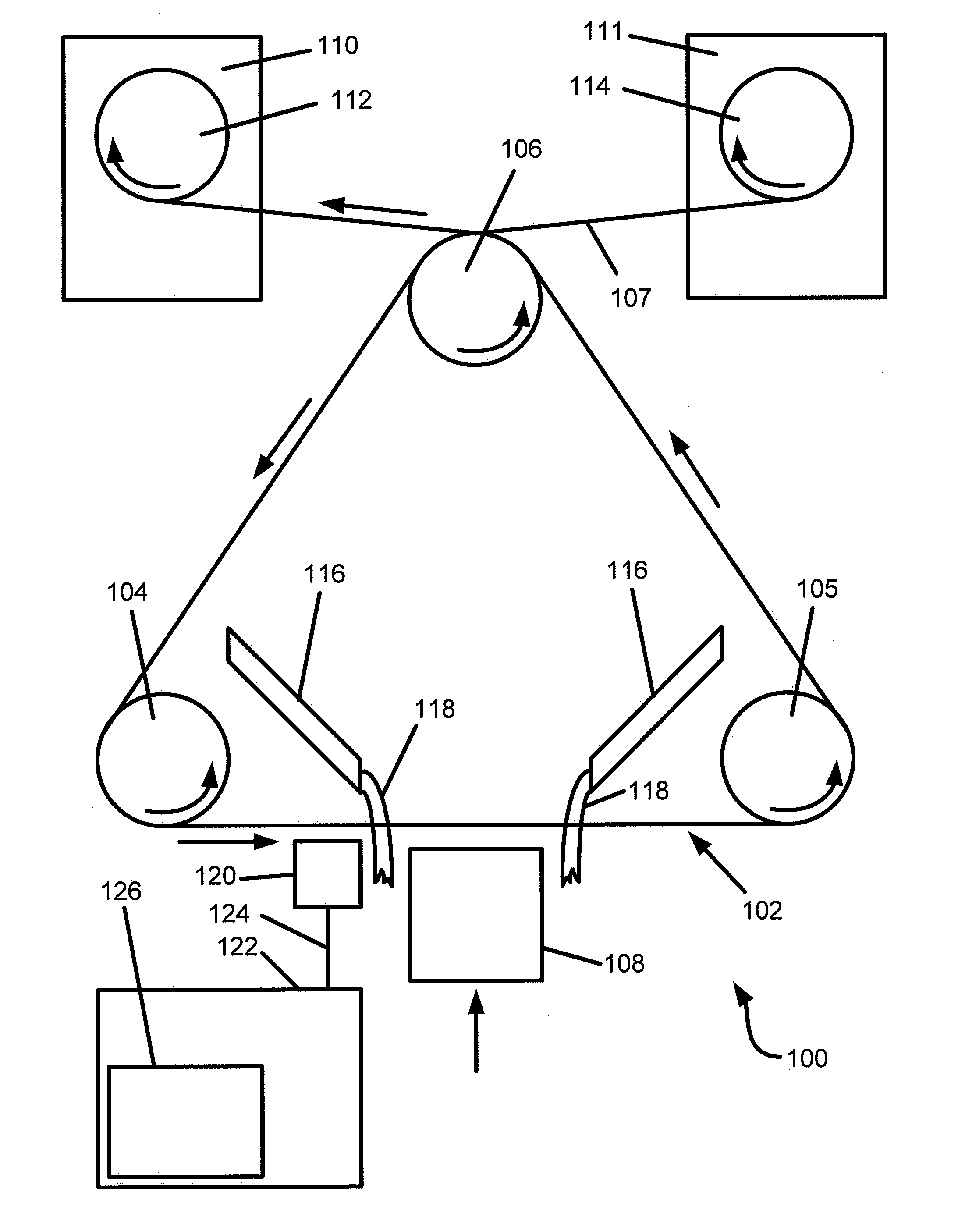
While the slurry in a slurry saw removes heat from the wire and the work piece during cutting, slurry-free wire saws do not inherently have a means to remove heat from the kerfs created during cutting.
Due to their small size the particles tend to stick to the cutting wire.
If not removed, the particles degrade the quality of cuts, and by inducing web vibration the particles increase the chance of ingot
structural failure.
For instance, particles on the cutting wire can scratch the surface of the wafers being cut.
This can lead to ingot
structural failure as well as a “thick-thin” effect (where adjacent wafers have larger and thinner thicknesses than the spacing between wire grooves).
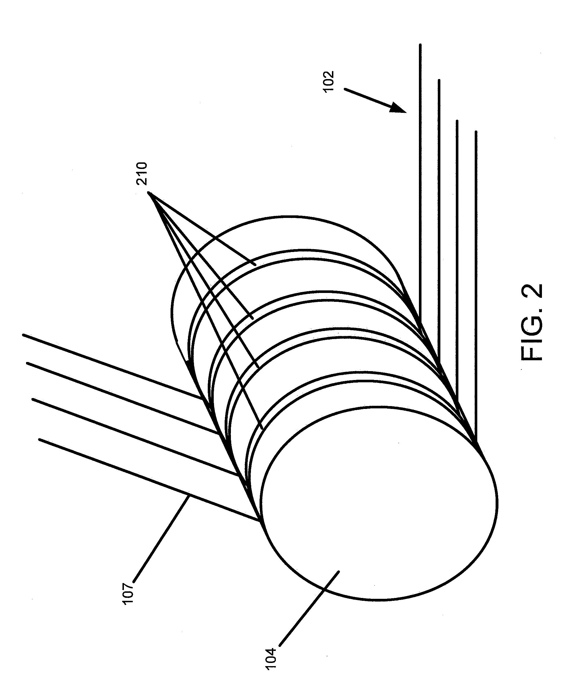
If one uses
ethylene glycol as the cleansing fluid to avoid the oxidation problem, then the
surface tension issues become prominent because of higher
viscosity, and the high
viscosity of the
ethylene glycol results in a poor job of cleansing, making the silicon particles stick to the wire, causing a reduction in the wire's cutting ability.

