
Eureka
For R&D, Eureka makes reading and utilizing patents & technical documents easy.
Eureka AIR
Designed for self-driven R&D workflows. Generate viable solutions, solve complex R&D challenges, empower your innovation with AI.

Eureka Materials
Designed for material experts only. Revolutionize your material R&D, from search, analyze, to developing new materials.

TechResearch
Generate reliable direction feasibility study reports for your R&D in just a few steps.

TechSeek
Discover and master advanced knowledge NOW. Basics, ideas, possibilities, all at once.

TechMind
As an expert in R&D Theories, TechMind can generates customized viable solutions instantly.

TechRisk
Analyze your overall solution with one click, know your potential R&D risks in advance.

TechMonitor
Get weekly tech updates, stay abreast of the latest tech innovations and key insights.
Method for producing optical component, optical component, and optical device
- Summary
- Abstract
- Description
- Claims
- Application Information
AI Technical Summary
Benefits of technology
Problems solved by technology
Method used
Image

Examples
specific examples
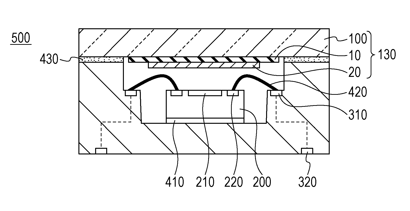
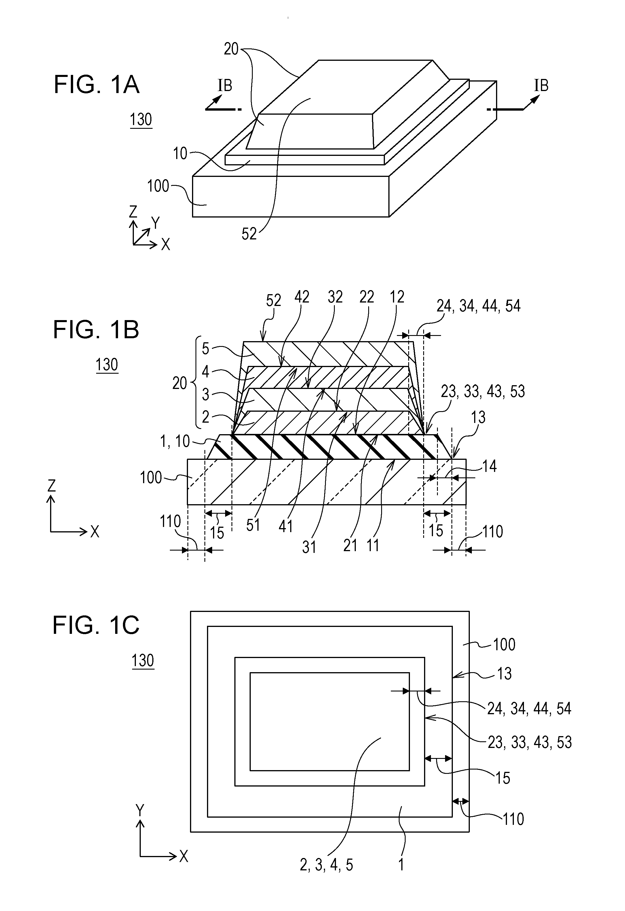
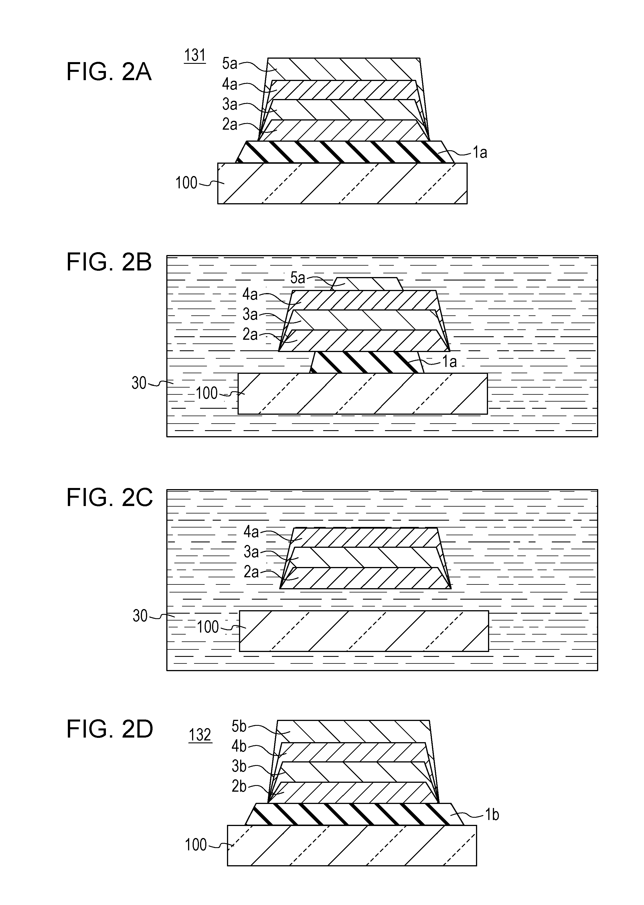
[0083]Regarding an optical component in which a first layer 1 that serves as a first film 10, and a second layer 2, a third layer 3, a fourth layer 4, and a fifth layer 5 that serve as a second film 20 are stacked on a substrate 100, samples 01 to 12 are prepared by changing conditions and immersed in a liquid 30. Evaluation results in this treatment will be described.
[0084]A quartz crystal plate Q or a borosilicate glass plate B having a square shape with a side of 4 cm and a thickness of 0.5 mm is used as a substrate 100. A first layer 1 having a thickness of 30 to 300 nm is formed on the substrate 100 so as to have a square shape Y with a side of 3 cm or a square shape N with a side of 2 cm by electron-beam heating evaporation. Furthermore, a second layer 2, a third layer 3, a fourth layer 4, and a fifth layer 5 each having a thickness of 10 to 200 nm are continuously formed on the first layer 1 in that order so as to have a square shape with a side of 2 cm by electron-beam heati...
PUM
 Abstract
Description
Claims
Application Information
 - R&D Engineer
- R&D Manager
- IP Professional
- Industry Leading Data Capabilities
- Powerful AI technology
- Patent DNA Extraction
Browse by: Latest US Patents, China's latest patents, Technical Efficacy Thesaurus, Application Domain, Technology Topic, Popular Technical Reports.
© 2024 PatSnap. All rights reserved.Legal|Privacy policy|Modern Slavery Act Transparency Statement|Sitemap|About US| Contact US: help@patsnap.com