Sensor-type package and fabrication method thereof

Inactive Publication Date: 2008-04-03
SILICONWARE PRECISION IND CO LTD
View PDF5 Cites 28 Cited by
  • Summary
  • Abstract
  • Description
  • Claims
  • Application Information

AI Technical Summary

Benefits of technology

[0023]The light-pervious body may have a planar size larger than a predefined planar size of the sensor-type package, such that side surfaces of the light-pervious body can be exposed by the cutting process, so as to facilitate the removal of the covering layer on the first surface of the light-pervious body and the portion of the encapsulant located on the covering layer. This ensures that light can pass through the light-pervious body to be captured by the sensor-type chip. Further, in order to prevent the light-pervious body (for example, made of glass) from cracking in the cutting process, the light-pervious body can firstly be cut by a bevel cutting technique along a predetermined cutting path corresponding to the planar size of the light-pervious body so as to form bevel edges on side surfaces of the light-pervious body, and then the molded structure is cut according to the predefined planar size of the sensor-type package.
[0024]The planar size of the light-pervious body can alternatively be slightly smaller than the predefined planar size of the sensor-type package, but has to be larger than a planar size of the sensor-type chip, such that the sensor-type chip can be protected by the light-pervious body. During the cutting process, the bevel cutting technique can be implemented to form bevel edges on a top surface of the encapsulant firstly, and then the molded structure can be cut according to the predefined package size of the sensor-type package. Afterwards, the covering layer on the first surface of the light-pervious body and the portion of the encapsulant located on the covering layer can be removed. Further, a protruding portion can be formed on the top surface of the encapsulant, such that a clamping device can be used to clamp the protruding portion so as to easily remove the covering layer and the portion of the encapsulant located on the covering layer.
[0025]To increase the adhesive force between the light-pervious body and the encapsulant and increase the adhesive force between the light-pervious body and the adhesive layer, a rough portion can be formed on the second surface of the light-pervious body at positions corresponding to the encapsulant and the adhesive layer.
[0026]The sensor-type package can be fabrica

Problems solved by technology

However, as the adhesive 16 is of high moisture absorptivity, in a high temperature environment of subsequent processes, the adhesive 16 tends to absorb moisture of the ambient and can cause a popcorn effect, thereby leading to delamination of the dam structure from the substrate and reducing the package reliability.
However, the above sensor-type package causes some significant drawbacks.
For example, a clamping force between the protruding portion and the substrate is not easy to control.
If the protruding portion cannot stably and closely abut against the substrate, the resin compound would easily flash through a gap between the protruding portion and the substrate and thereby contaminate the chip-mounting and wire-bonding areas.
On the other hand, if the protruding portion is too tightly pressed against the substrate, the substrate would be damaged.
Further, the mold needs to have its protruding portion sized according to the size of the predefined areas of the substrate and is not cost effective to fabricate.
In other words, if the size of the predefined areas of the substrate is changed, a new mold having an appropriate protruding portion should be prepared, thereby undesirably increasing the fabrication cost and complicating the fabrication

Method used


Image

  • Sensor-type package and fabrication method thereof
  • Sensor-type package and fabrication method thereof
  • Sensor-type package and fabrication method thereof

Examples


Example

First Embodiment

[0042]FIGS. 5A to 5F are schematic diagrams showing a sensor-type package and a fabrication method thereof according to a first embodiment of the present invention. In this embodiment, the sensor-type package is fabricated in a batch-type manner.

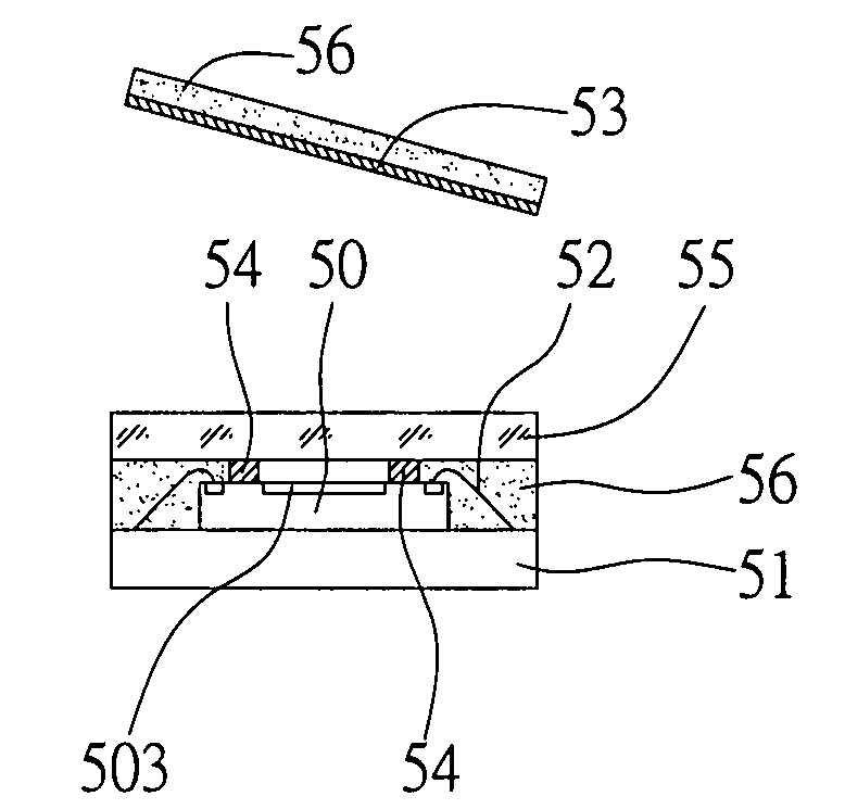
[0043]As shown in FIG. 5A, a substrate module plate 51 A comprising a plurality of substrates 51 is provided, and a sensor-type chip 50 is mounted on each of the substrates 51. A planar size of the sensor-type chip 50 is smaller than a planar size of the substrate 51 that corresponds to a predefined package size. The substrate module plate 51. A may have the plurality of substrates 51 arranged in a matrix or in a strip. The sensor-type chip 50 has an active surface 501 and a non-active surface 502 opposed to the active surface 501, wherein the active surface 501 is formed with a sensor area 503 and a plurality of bonding pads 504 thereon. The non-active surface 502 of the sensor-type chip 50 is attached to the corresponding s...

Example

Second Embodiment

[0051]FIGS. 6A to 6C are schematic diagrams showing a sensor-type package and a fabrication method thereof according to a second embodiment of the present invention. The second embodiment is similar to the above first embodiment, and differs from the first embodiment primarily in that, when the sensor area is very close to the bonding pads of the sensor-type chip, for example, with a distance therebetween being smaller than 300 μm, the adhesive layer on the second surface of the light-pervious body cannot be disposed between the sensor area and the bonding pads; instead, the adhesive layer is attached to the bonding pads of the sensor-type chip and encapsulates end portions of the bonding wires connected to the sensor-type chip.

[0052]As shown in FIG. 6A, a sensor-type chip 50 is mounted on each of the substrates 51, wherein the sensor-type chip 50 is formed with a sensor area 503 and bonding pads 504 on an active surface thereof. The sensor-type chip 50 is attached ...

Example

Third Embodiment

[0057]FIGS. 7A to 7D are schematic diagrams showing a sensor-type package and a fabrication method thereof according to a third embodiment of the present invention. The third embodiment is similar to the above embodiments, and differs from the above embodiments primarily in that, when the light-pervious body has a size larger than the predefined package size, a cutting path would pass through the light-pervious body, and a bevel cutting technique is employed to form bevel edges on side surfaces of the light-pervious body so as to prevent the light-pervious body (made of such as glass) from cracking during the cutting process.

[0058]As shown in FIGS. 7A and 7B, after mounting the sensor-type chips 50 on the substrates 51, forming the bonding wires 52, and attaching the light-pervious bodies 55 to the sensor-type chips 50, and performing the molding process to form the encapsulant 56 on the substrates 51, a bevel cutting technique is implemented to cut the encapsulant 5...


PUM


Abstract

A sensor-type package and a fabrication method thereof are provided. A sensor-type chip is mounted on a substrate and is electrically connected to the substrate via bonding wires. A light-pervious body is attached to the sensor-type chip, and has one surface covered with a covering layer and another surface formed with an adhesive layer. An encapsulant encapsulates the light-pervious body. As an adhesive force between the covering layer and the encapsulant is greater than that between the covering layer and the light-pervious body, the covering layer and a portion of the encapsulant located on the covering layer can be concurrently removed, such that the light-pervious body is exposed and light can pass through the light-pervious body to be captured by the sensor-type chip. The above arrangement eliminates the need of using a dam structure as in the prior art and provides a compact sensor-type package with improved fabrication reliability.

Description

FIELD OF THE INVENTION[0001]The present invention relates generally to semiconductor packages and fabrication methods thereof, and more particularly, to a sensor-type package and a method of fabricating the sensor-type package.BACKGROUND OF THE INVENTION[0002]Conventionally, to fabricate an image sensor package, a sensor-type chip is mounted on a chip carrier and is electrically connected to the chip carrier via a plurality of bonding wires, and then a glass member is provided above the sensor-type chip, allowing the sensor-type chip to capture image light passing through the glass member. Such an image sensor package is generally assembled into an external device, such as a printed circuit board, for use in various electronic products such as a digital camera, digital video camera, mobile phone, finger print sensor, and the like.[0003]Referring to FIG. 1, a sensor-type package disclosed by U.S. Pat. No. 6,060,340 is shown. A dam structure 13 is formed and is attached to a substrate...

Claims


Application Information

Patent Timeline
IPC IPC(8): H01L31/0203H01L21/02
CPCH01L24/97H01L2924/01033H01L27/14683H01L2224/48091H01L2224/48227H01L2224/97H01L2924/01082H01L2924/15311H01L2924/16195H01L27/14618H01L2924/01005H01L2224/85H01L2924/00014
Inventor CHANG, TSE-WENCHAN, CHANG-YUEHHUANG, CHIEN-PINGHUANG, CHIH-MINGHSIAO, CHENG-HSU
Owner SILICONWARE PRECISION IND CO LTD
Why Eureka
Try Eureka