

Method for determining an optimal voltage pulse for programming a flash memory cell
- Summary
- Abstract
- Description
- Claims
- Application Information
AI Technical Summary
Benefits of technology
Problems solved by technology
Method used
Image

Examples
Embodiment Construction
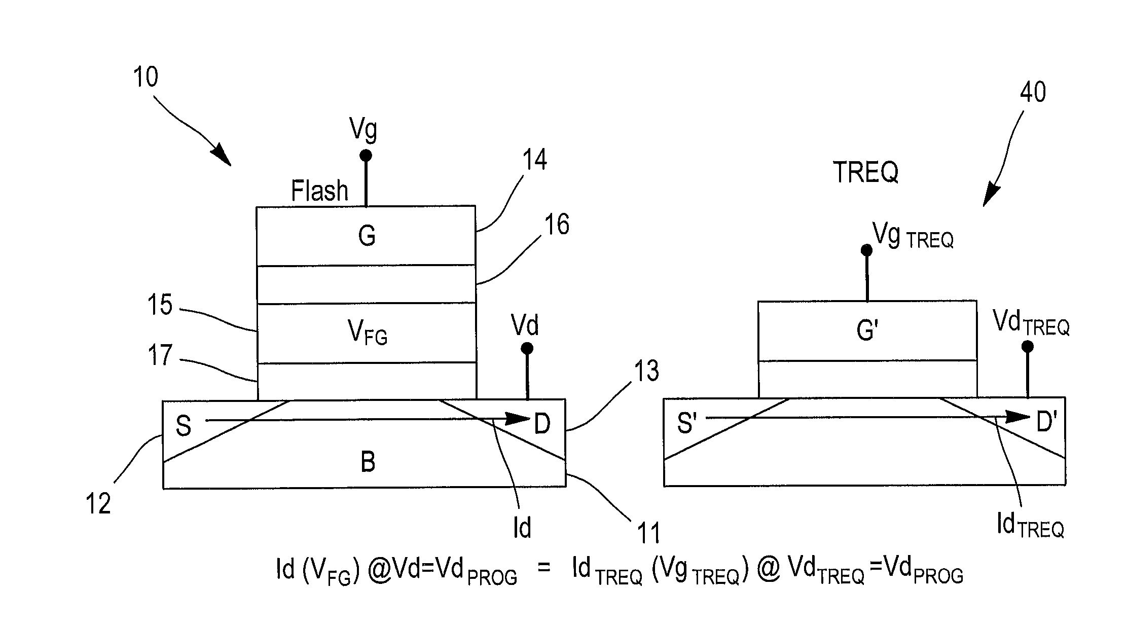
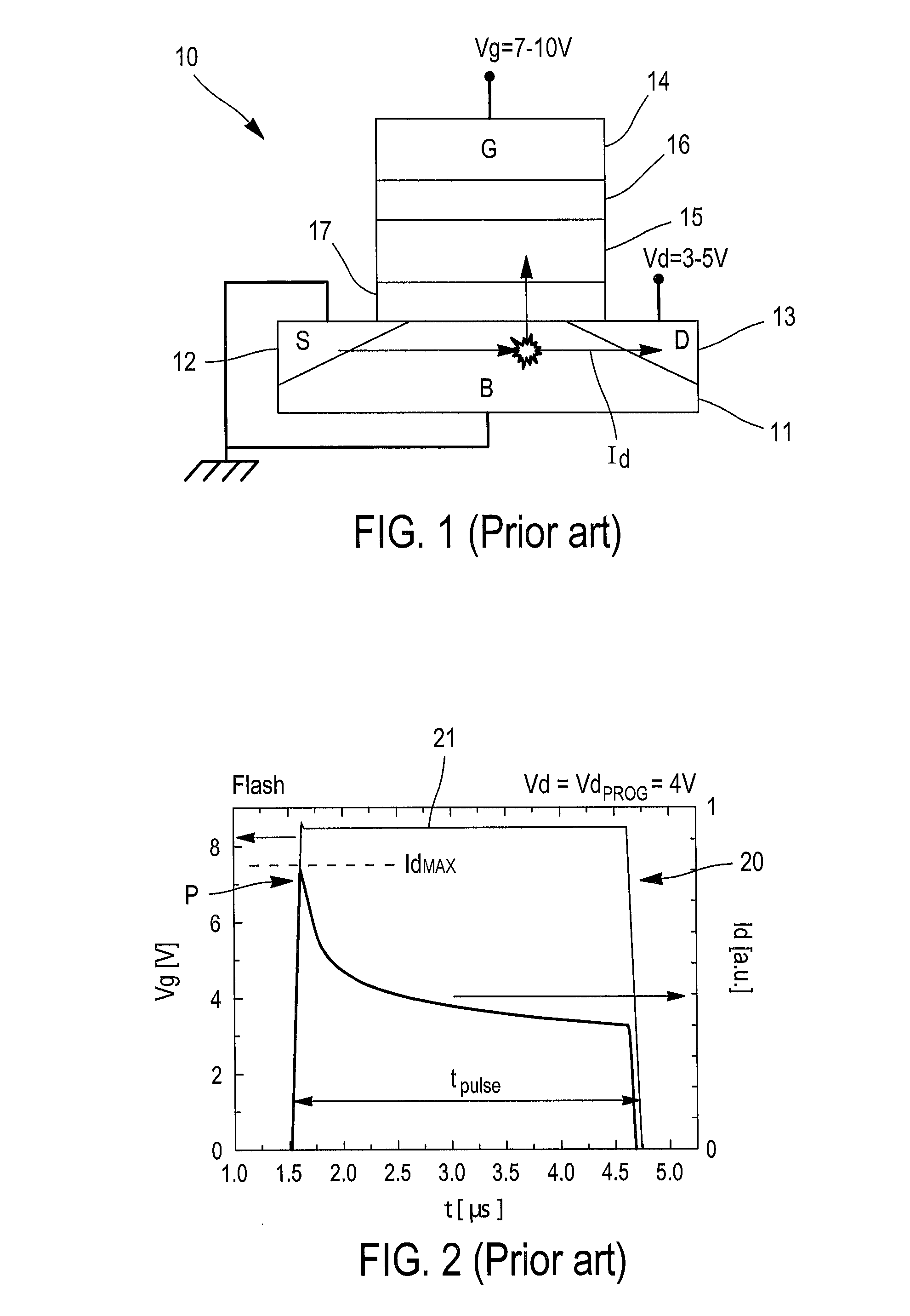
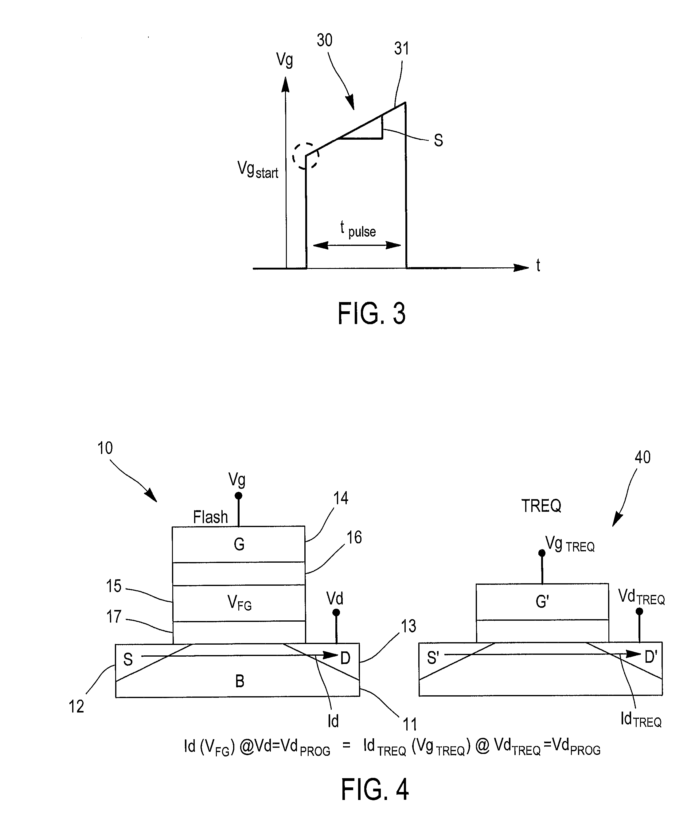
[0049]In the description that follows, a unit EEPROM-Flash memory (i.e. of a capacity of 1 bit) of NOR type is called “flash memory cell”. This cell may be embedded in a test circuit, to develop and qualify EEPROM-Flash technology, or constitute the base of a flash memory circuit. A flash memory circuit, or memory array, includes a plurality of these memory cells arranged in lines and columns. NOR-type EEPROM-Flash memory circuits today equip numerous electronic devices, for example mobile telephones, for storing all types of information, in particular programs.
[0050]As described previously (FIG. 1), a flash memory cell is provided with a transistor including a control gate, a floating gate, drain and source regions formed in a semiconductor substrate. The control gate, the drain, the source and the substrate constitute control electrodes, noted respectively G, D, S and B. These electrodes allow to bias the transistor to carry out programming (or writing), erasing or reading operati...
PUM
 Abstract
Description
Claims
Application Information