Organic electroluminescent display panel

a technology of electroluminescent display panels and electroluminescent light, which is applied in the direction of organic semiconductor devices, electrical devices, semiconductor devices, etc., can solve the problems of deteriorating display quality and reducing the purity of luminescent colors, and achieve the effect of enhancing display quality and suppressing the influence of color mixtures

Inactive Publication Date: 2016-11-03
SHARP KK
View PDF20 Cites 3 Cited by
  • Summary
  • Abstract
  • Description
  • Claims
  • Application Information

AI Technical Summary

Benefits of technology

[0022]The present invention can provide an organic EL display panel that can s...

Problems solved by technology

This vapor deposition technique, however, may cause color mixture between adjacent pix...

Method used


Image

  • Organic electroluminescent display panel
  • Organic electroluminescent display panel
  • Organic electroluminescent display panel

Examples


embodiment 1

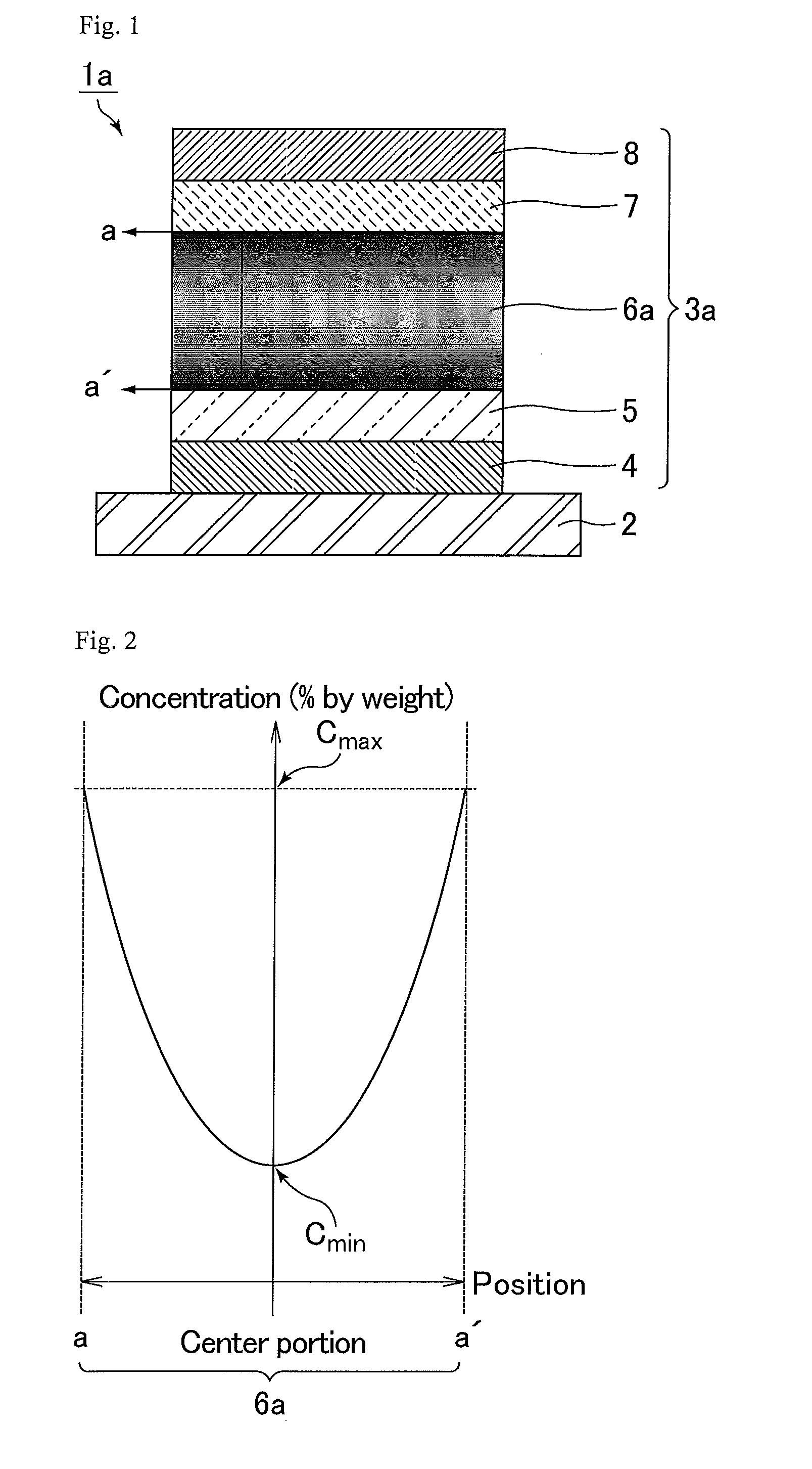
[0036 relates to an organic EL display panel including an anode, a light-emitting portion, and a cathode in the order from the substrate side, and to a configuration in which the concentration of the luminescent dopant material is at a local maximum in the vicinities of the interfaces on the anode side and on the cathode side, and is symmetrically distributed, in the thickness direction of the light-emitting portion.

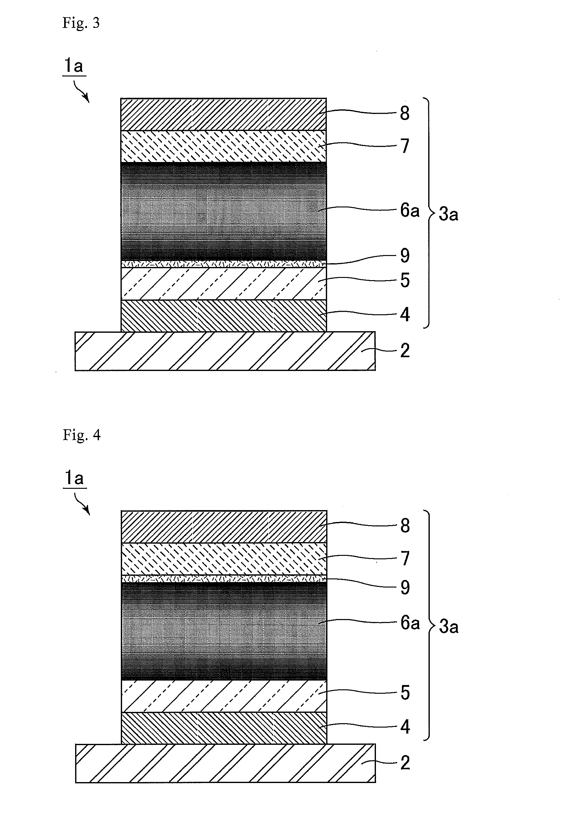
[0037]FIG. 1 is a schematic cross-sectional view illustrating a pixel in an organic EL display panel of Embodiment 1. Here, the pixel illustrated in FIG. 1 corresponds to one pixel in an organic EL display panel in which the luminescent colors of adjacent light-emitting portions are different from each other as already described with reference to FIGS. 8 to 11. As long as the luminescent colors of adjacent light-emitting portions are different from each other, the order of disposing the light-emitting portions and the kind of the luminescent colors are not particularly l...

embodiment 2

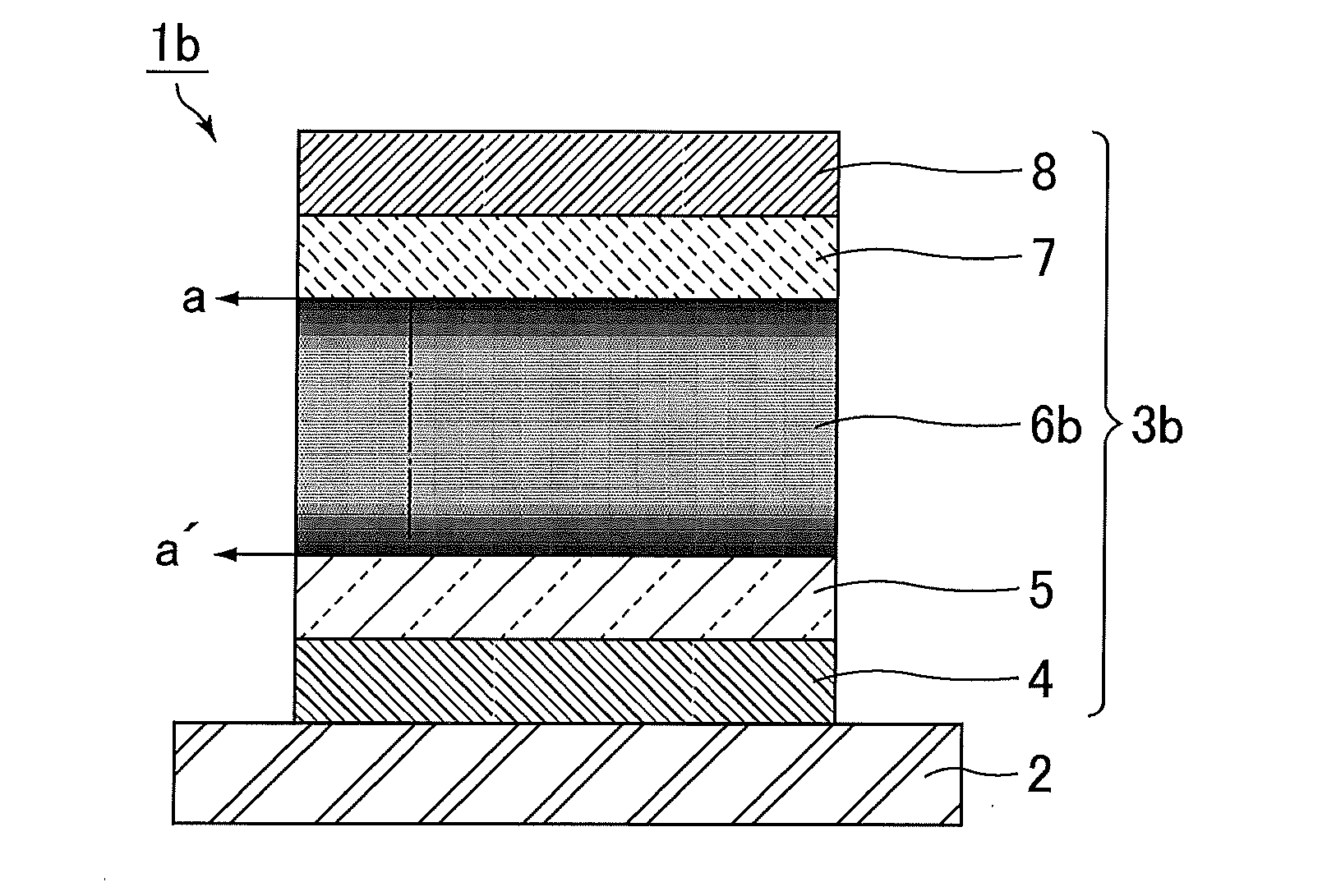
[0058]FIG. 5 is a schematic cross-sectional view illustrating a pixel in an organic EL display panel of As illustrated in FIG. 5, an organic EL display panel 1b includes the substrate 2 and an organic EL element 3b disposed on the substrate 2. The organic EL element 3b includes the anode 4, the hole transport layer 5, a light-emitting portion 6b, the electron transport layer 7, and the cathode 8 in the order from the substrate 2 side.

[0059]Next, the concentration of the luminescent dopant material constituting the light-emitting portion 6b is described with reference to FIG. 6. FIG. 6 is a graph showing the concentration of a luminescent dopant material corresponding to the a-a′ line in FIG. 5. The vertical axis in FIG. 6 indicates the concentration of the luminescent dopant material and the horizontal axis indicates the position on the a-a′ line in FIG. 5. As illustrated in FIG. 6, the concentration of the luminescent dopant material has the following characteristics (C) and (D) i...


PUM


Abstract

The organic EL display panel includes: a substrate; and an organic electroluminescent element disposed on the substrate, the organic electroluminescent element including, in the given order: an anode; a light-emitting layer; and a cathode, the light-emitting layer including multiple light-emitting portions, the multiple light-emitting portions each providing a luminescent color different from the luminescent color of the adjacent light-emitting portion, the multiple light-emitting portions each containing a luminescent dopant material, the concentration of the luminescent dopant material in each light-emitting portion changing in the thickness direction of the light-emitting portion and being at a local maximum in the vicinity of a first interface on the anode side and in the vicinity of a second interface on the cathode side, the local maximum in each light-emitting portion being 20% by weight or higher of the total weight of the light-emitting portion.

Description

CROSS-REFERENCE TO RELATED APPLICATIONS[0001]This application is a National Phase filing under 35 USC 371 application of International Application No. PCT / JP2014 / 072574, filed on Aug. 28, 2014, which claims priority to Japanese Application No. 2014-004327, filed on Jan. 14, 2014, each of which is hereby incorporated by reference in the present disclosure in their entirety.FIELD OF THE INVENTION[0002]The present invention relates to organic electroluminescent display panels (hereinafter, also referred to as “organic EL display panels”). More specifically, the present invention relates to an organic EL display panel including light-emitting portions, wherein the luminescent colors of adjacent light-emitting portions are different from each other.BACKGROUND OF THE INVENTION[0003]Organic electroluminescent elements (hereinafter, also referred to as “organic EL elements”) utilizing electroluminescence of organic materials have drawn attention as display elements used for thin display dev...

Claims


Application Information

Patent Timeline
IPC IPC(8): H01L27/32
CPCH01L27/3211H01L2251/5346H10K59/35H10K50/11H10K2101/80
Inventor KAWATO, SHINICHIOCHI, TAKASHIINOUE, SATOSHIKOBAYASHI, YUHKIMATSUNAGA, KAZUKIKIKUCHI, KATSUHIRO
Owner SHARP KK
Why Eureka
Try Eureka