Semiconductor device having contact plug and method of forming the same

Active Publication Date: 2016-11-10
SAMSUNG ELECTRONICS CO LTD
View PDF1 Cites 5 Cited by
  • Summary
  • Abstract
  • Description
  • Claims
  • Application Information

AI Technical Summary

Benefits of technology

The inventive concepts provide a semiconductor device with better electrical properties.

Problems solved by technology

As semiconductor devices become more highly integrated, it typically becomes more difficult to reduce or substantially prevent leakage current from contact plugs.
Since the contact plugs are typically formed on the lower patterns at various intervals, various problems, such as an increase in leakage current, may occur.

Method used


Image

  • Semiconductor device having contact plug and method of forming the same
  • Semiconductor device having contact plug and method of forming the same
  • Semiconductor device having contact plug and method of forming the same

Examples


Embodiment Construction

[0065]Advantages and features of the example inventive concepts and methods thereof will be made apparent with reference to the accompanying figures and the example embodiments to be described below in detail. However, the inventive concepts should not be limited to the example embodiments set forth herein and may be construed as various embodiments in different forms. Rather, these example embodiments are provided so that disclosure of the inventive concepts is thorough and complete, and fully conveys the inventive concepts to those of ordinary skill in the art. The inventive concepts are defined by the appended claims.

[0066]The terminology used herein is only intended to describe example embodiments of the inventive concepts and not intended to limit the scope of the inventive concepts. As used herein, the singular forms “a,”“an,” and “the” are intended to include the plural forms as well, unless specifically indicated otherwise. The terms “comprises” and / or “comprising” that are ...


PUM


Abstract

A semiconductor device includes merged contact plugs. A multi-fin active having N sub-fins is formed in a substrate. A contact plug is formed on the impurity areas. N is an integer between about eight (8) and about one thousand (1000). The N sub-fins include a first sub-fin formed in the outermost portion of the multi-fin active and a second sub-fin formed near the first sub-fin. A straight line perpendicular to a surface of the substrate and passes through a virtual bottom edge of the contact plug is disposed between the first sub-fin and the second sub-fin, or through the second sub-fin. The virtual bottom edge of the contact plug is defined at a cross point of a correlation line extending on a side surface of the contact plug and a horizontal line in contact with a lowermost end of the contact plug and parallel to the surface of the substrate.

Description

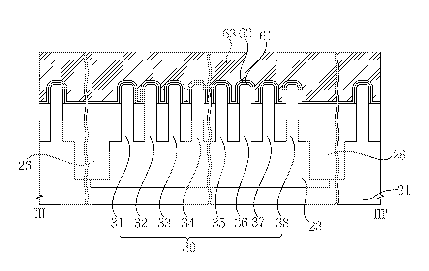
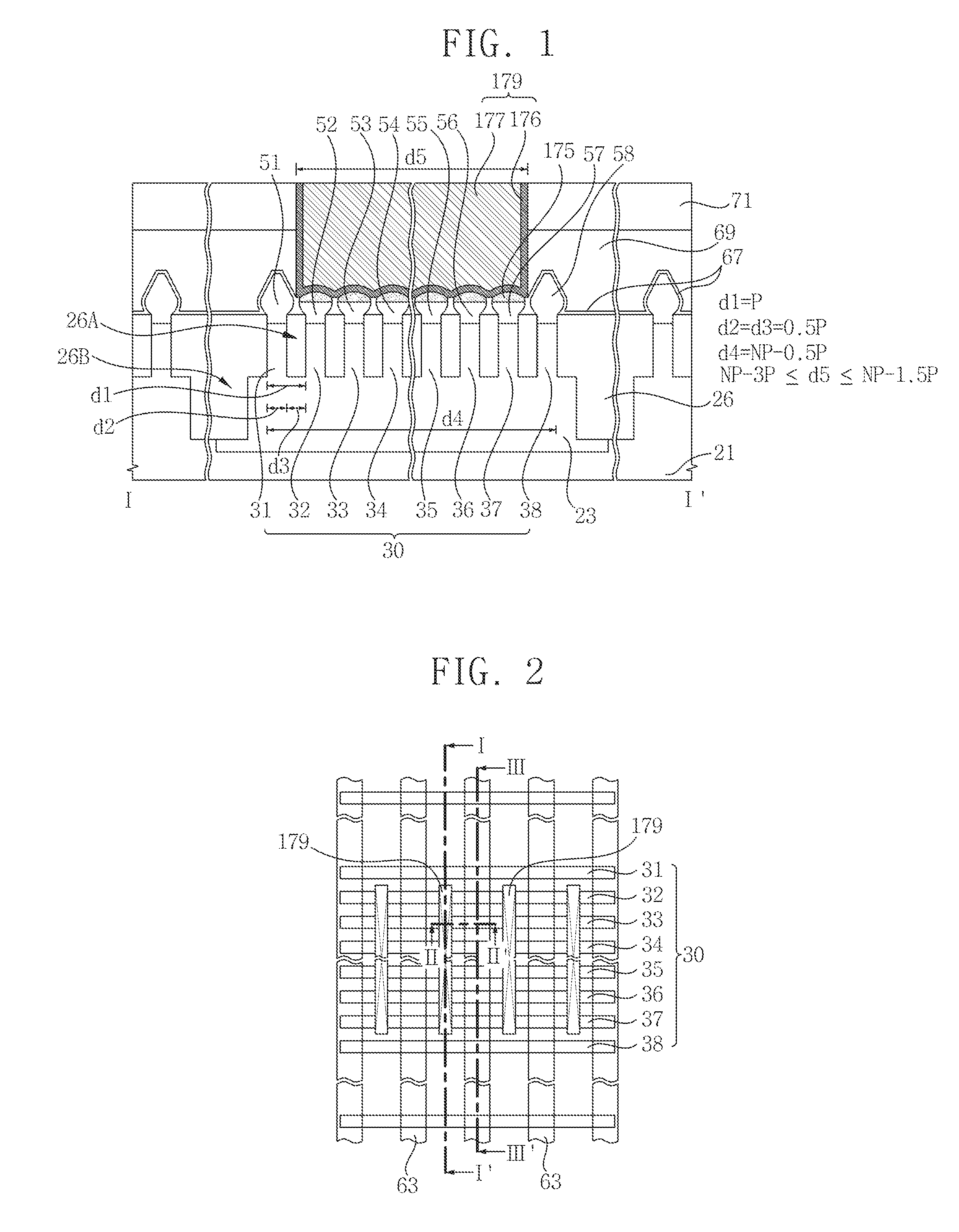
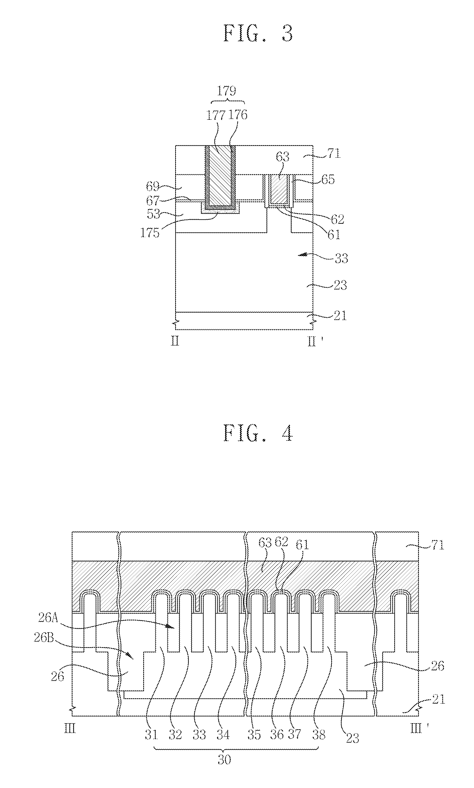
CROSS-REFERENCE TO RELATED APPLICATION[0001]This application claims priority under 35 U.S.C. §119 to Korean Patent Application No. 10-2015-0062534 filed on May 4, 2015, the disclosure of which is hereby incorporated by reference in its entirety.BACKGROUND[0002]1. Field[0003]Embodiments of the inventive concepts relate to a semiconductor device including merged contact plugs, and / or a method of forming the same.[0004]2. Description of Related Art[0005]As semiconductor devices become more highly integrated, it typically becomes more difficult to reduce or substantially prevent leakage current from contact plugs. The contact plugs serve to provide electrical connections between lower patterns and upper interconnections. The lower patterns may be arranged at various intervals to configure a circuit. Since the contact plugs are typically formed on the lower patterns at various intervals, various problems, such as an increase in leakage current, may occur.SUMMARY[0006]Embodiments of the i...

Claims


Application Information

Patent Timeline
IPC IPC(8): H01L27/088H01L29/06H01L23/532H01L27/02H01L23/528
CPCH01L27/0886H01L27/0207H01L29/0649H01L23/53209H01L23/528H01L23/535H01L29/1033H01L21/823431H01L21/823475H01L27/0629H01L29/861H01L29/0657H01L29/41791H01L27/0924H01L23/5283
Inventor MOON, HYERIMCHOI, MYOUNGHUN
Owner SAMSUNG ELECTRONICS CO LTD
Why Eureka
Try Eureka