Metal interconnection structure of a semiconductor device having low resistance and method of fabricating the same

Active Publication Date: 2006-10-26
SK HYNIX INC
View PDF3 Cites 5 Cited by
  • Summary
  • Abstract
  • Description
  • Claims
  • Application Information

AI Technical Summary

Benefits of technology

[0009] Therefore, the present invention has been made in view of the above problems, and it is an object of the present invention to provide a metal interconnection structure of a semiconductor device having relatively low resistance in order to improve electrical properties thereof.

Problems solved by technology

For this purpose, complicated circuits of the devices have been implemented by reducing the contact length and contact resistance between devices via formation of metal interconnection as a multi-layer structure.
However, frequency of usage of the metal contact plug is also increased in metal interconnection structures showing a trend toward use of multi-layer structures and as a result, electrical properties of devices are gradually degraded due to a high specific resistance of tungsten.

Method used


Image

  • Metal interconnection structure of a semiconductor device having low resistance and method of fabricating the same
  • Metal interconnection structure of a semiconductor device having low resistance and method of fabricating the same
  • Metal interconnection structure of a semiconductor device having low resistance and method of fabricating the same

Examples


Embodiment Construction

[0042] Now, preferred embodiments of the present invention will be described in more detail with reference to the accompanying drawings, such that those skilled in the art can easily practice the present invention.

[0043] In the drawings, thicknesses of various layers and regions are exaggerated for clarity. Like numbers refer to like elements throughout the specification and drawings.

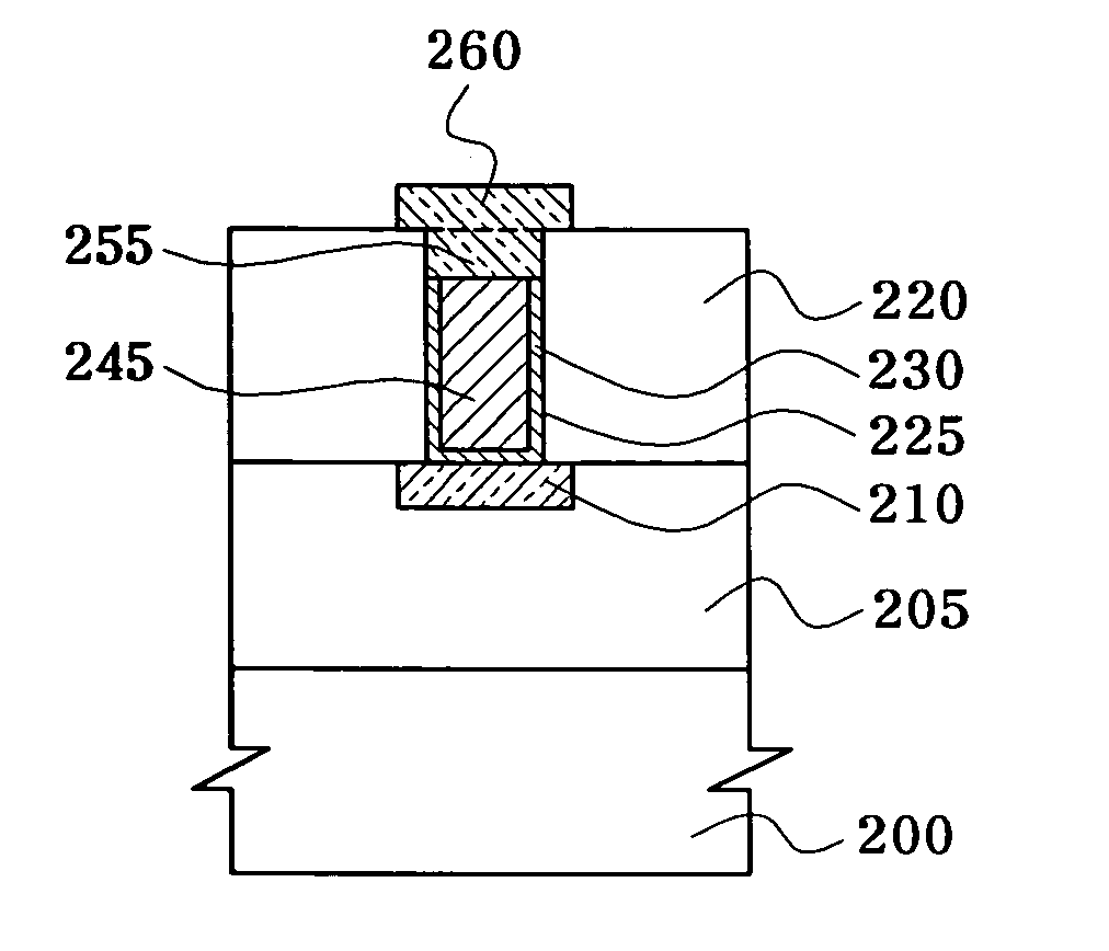
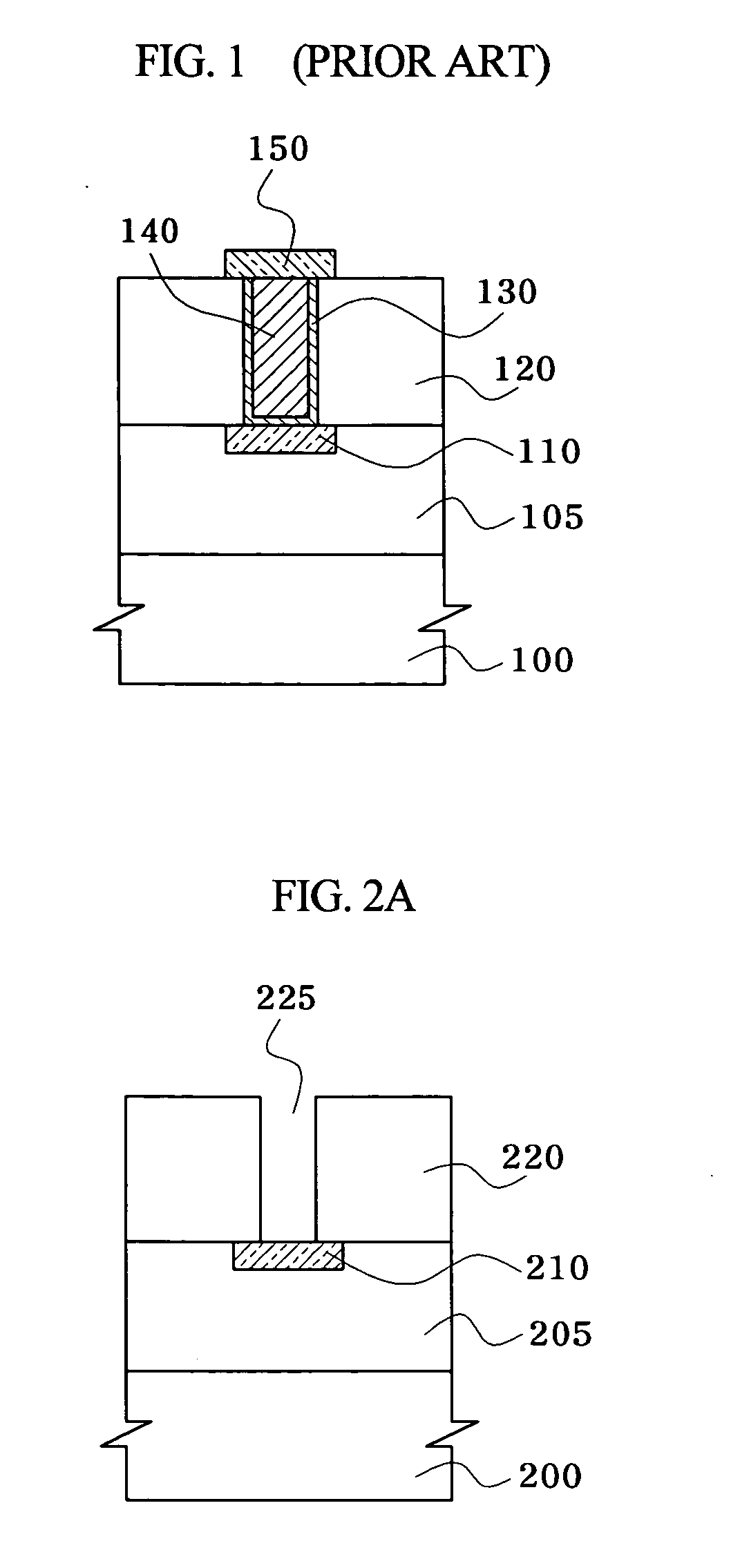
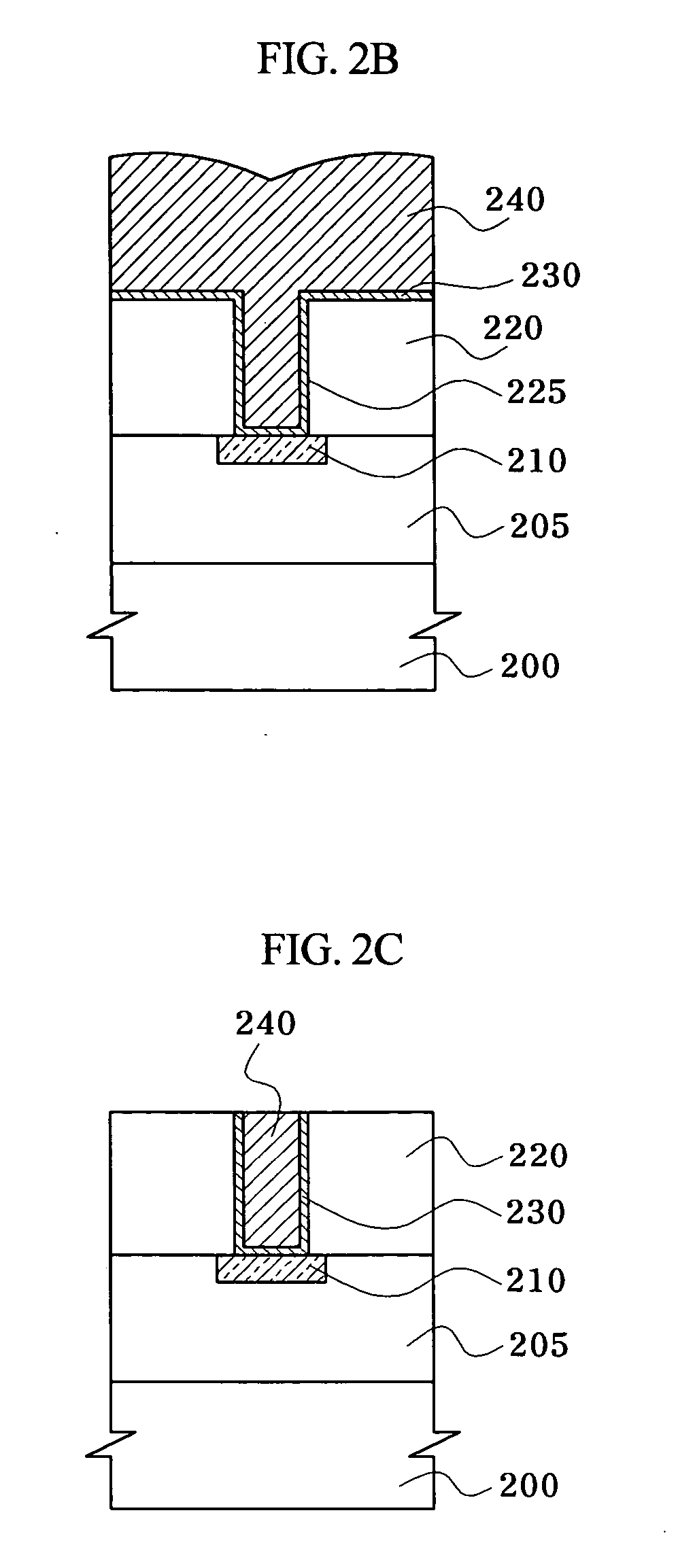
[0044]FIG. 2f is a cross-sectional view showing a metal interconnection structure of a semiconductor device in accordance with the present invention. Referring to FIG. 2f, a first metal film pattern 210 is disposed on an upper part of an insulation film 205 of a semiconductor substrate 200. An intermetallic dielectric film 220 having a via-hole 225 exposing an upper surface of the first metal film pattern 210 is disposed on the first metal film pattern 210 and insulation film 205. A barrier layer 230 is disposed within the via-hole 225 and a first metal contact plug 245 is disposed on the barrier laye...


PUM


Abstract

Provided is a metal interconnection structure of a semiconductor device, comprising a first metal film pattern disposed on an upper part of an insulation film of a semiconductor substrate; an intermetallic dielectric film having a metal contact plug in which a barrier layer, a metal film for contact plug and a second metal film are sequentially disposed, on the first metal film pattern; and a second metal film pattern disposed on the metal contact plug and intermetallic dielectric film and connected to the metal contact plug.

Description

BACKGROUND OF THE INVENTION [0001] 1. Field of the Invention [0002] The present invention relates to a semiconductor device and a method of fabricating the same, and more particularly to a metal interconnection structure of a semiconductor device having low resistance and a method of fabricating the same. [0003] 2. Description of the Related Art [0004] Recently, the increased degree of integration of semiconductor memory devices has led to miniaturization and high densification thereof. However, such high integration enables reduction of the device size and integration of the circuits having sophisticated functions into the device and as a result, increased lengths of signal lines providing connection between the devices. Therefore, reduction of a signal line length is absolutely necessary for enhancing operating speed of integrated circuits. For this purpose, complicated circuits of the devices have been implemented by reducing the contact length and contact resistance between devi...

Claims


Application Information

Patent Timeline
IPC IPC(8): H01L21/4763
CPCH01L21/76877H01L21/28
Inventor RYU, IN CHEOLJIN, SUNG-GON
Owner SK HYNIX INC
Why Eureka
Try Eureka