Active device and manufacturing method thereof

Inactive Publication Date: 2015-04-16
E INK HLDG INC
View PDF5 Cites 3 Cited by
  • Summary
  • Abstract
  • Description
  • Claims
  • Application Information

AI Technical Summary

Benefits of technology

The invention relates to an active device. The invention includes a process where a first passivation layer and a second passivation layer are formed on a channel layer. This process helps to protect the second passivation layer from damage during the formation of other layers. The second passivation layer also helps to isolate external influences such as moisture and oxygen from the channel layer. The process also allows the source and drain to be positioned in a way that improves their electrical properties and performance.

Problems solved by technology

Accordingly, it is overly difficult to control an etching process for forming the source and the drain, thereby influencing a performance and a reliability of the bottom gate TFT.

Method used


Image

  • Active device and manufacturing method thereof
  • Active device and manufacturing method thereof
  • Active device and manufacturing method thereof

Examples


Embodiment Construction

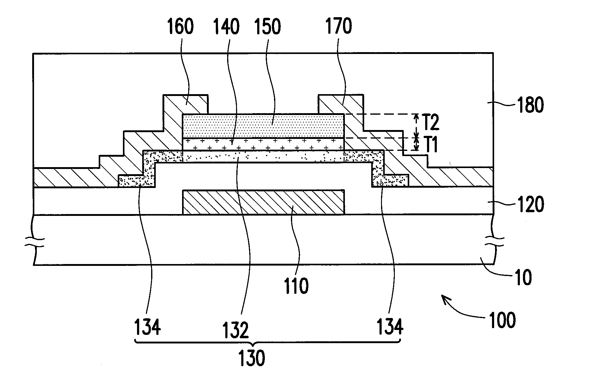
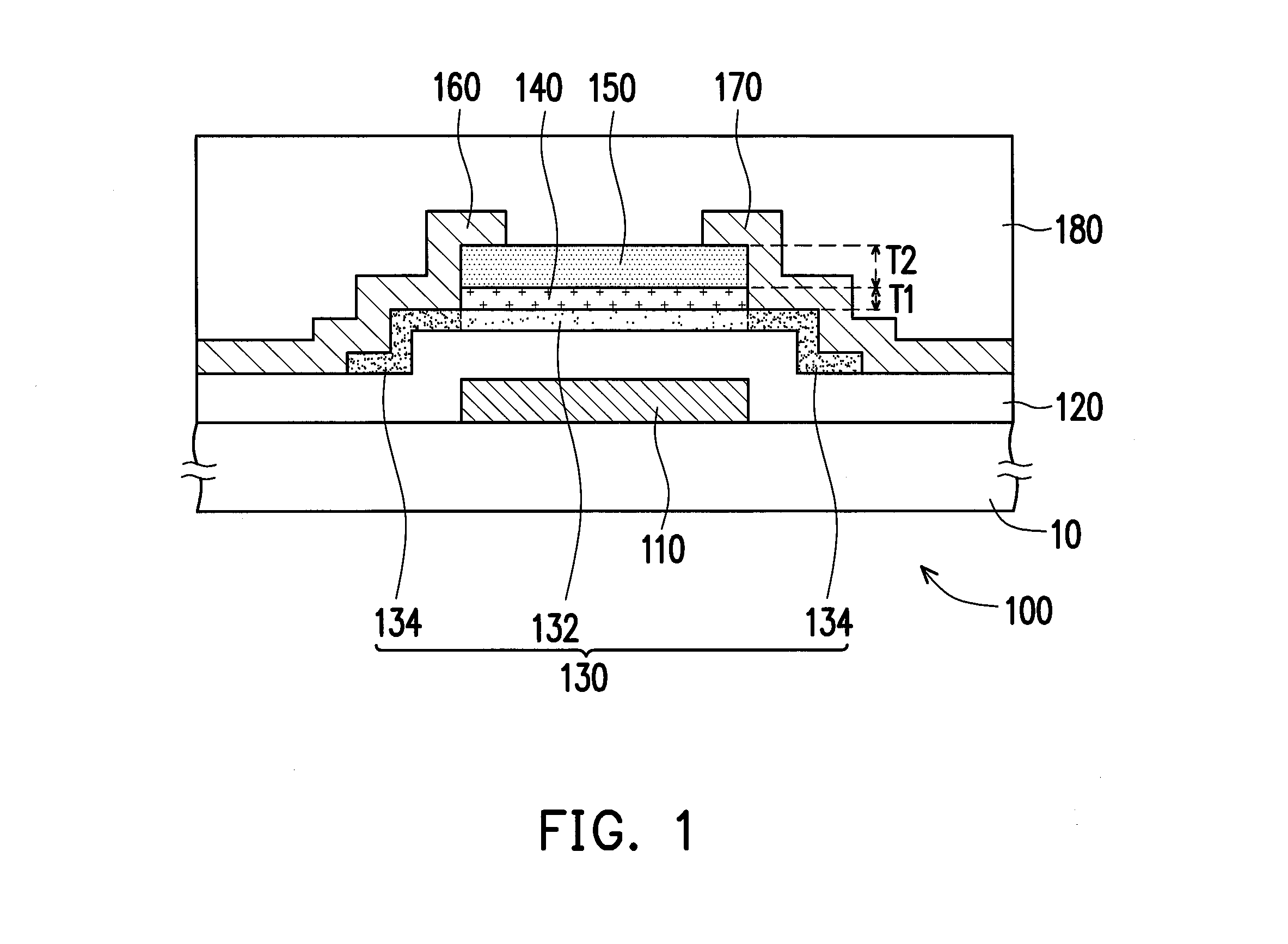
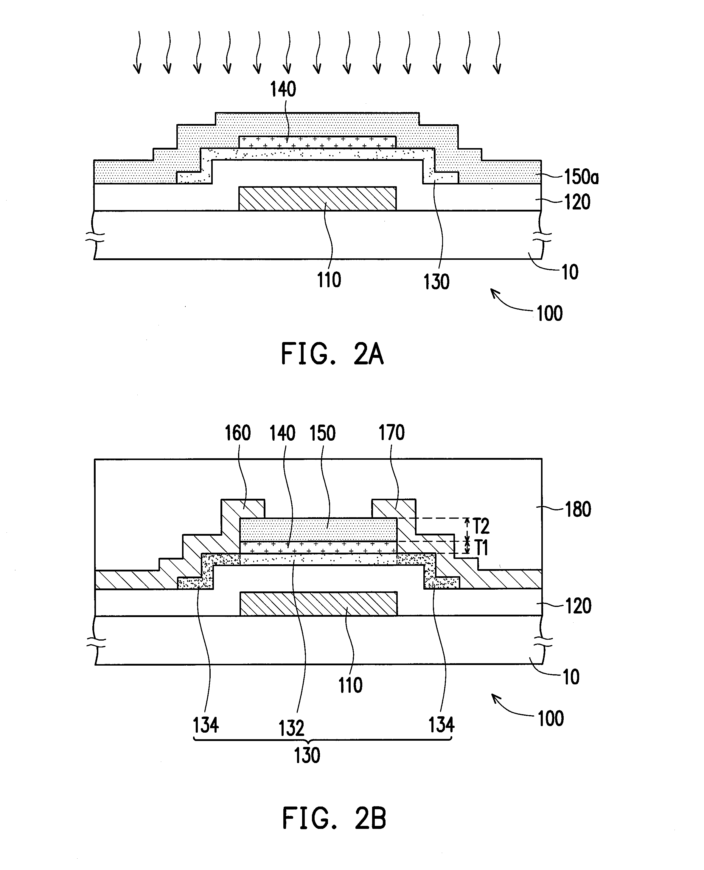
[0028]FIG. 1 is a schematic cross-sectional view of an active device according to an embodiment of the invention. Referring to FIG. 1, in the present embodiment, an active device 100 is disposed on a substrate 10, and the active device 100 includes a gate 110, a gate insulation layer 120, a channel layer 130, a first passivation layer 140, a second passivation layer 150, a source 160 and a drain 170. Herein, the substrate 10 is a glass substrate for example, but the invention is not limited thereto.

[0029]More specifically, the gate insulation layer 120 is disposed on the substrate 10, and covers the gate 110 and a portion of the substrate 10 exposed by the gate 110. The channel layer 130 is disposed on the gate insulation layer 120, and has a semiconductor section 132 and a conductive section 134 located around the semiconductor section 132. The semiconductor section 132 is disposed corresponding to the gate 110. The first passivation layer 140 is disposed on the channel layer 130 a...


PUM


Abstract

An active device includes a gate, a gate insulation layer, a channel layer, a first passivation layer, a second passivation layer, a source and a drain. The gate insulation layer is disposed on the substrate and covers the gate. The channel layer is disposed on the gate insulation layer and has a semiconductor section disposed corresponding to the gate and a conductive section located around the semiconductor section. The first passivation layer is disposed on the channel layer and covers the semiconductor section. The second passivation layer is disposed on and covers the first passivation layer. The source and the drain are disposed on the gate insulation layer, and extended along peripheries of the conductive section, the first and the second passivation layers to be disposed on the second passivation layer. A portion of the second passivation layer is exposed between the source and the drain.

Description

CROSS-REFERENCE TO RELATED APPLICATION[0001]This application claims the priority benefit of Taiwan application serial no. 102136819, filed on Oct. 11, 2013. The entirety of the above-mentioned patent application is hereby incorporated by reference herein and made a part of this specification.BACKGROUND OF THE INVENTION[0002]1. Field of the Invention[0003]The invention relates to a semiconductor device and a manufacturing method thereof, and more particularly, to an active device and a manufacturing method thereof.[0004]2. Description of Related Art[0005]In a typical thin film transistor (TFT) array substrate, amorphous silicon (a-Si) TFTs or low-temperature poly-silicon TFTs are usually used as switching elements for various sub-pixels. In recent years, studies have shown that an oxide semiconductor TFT has higher carrier mobility than the a-Si TFT, and the oxide semiconductor TFT is advantageous over the low-temperature poly-silicon TFT in large-area and low-cost fabrication. There...

Claims


Application Information

Patent Timeline
IPC IPC(8): H01L29/786H01L29/66
CPCH01L29/7869H01L29/66969H01L29/78606
Inventor YANG, CHIH-HSIANGSHINN, TED-HONGCHEN, WEI-TSUNGWU, HSING-YI
Owner E INK HLDG INC
Why Eureka
Try Eureka