Method for forming crack-stopping structures

a crack-stopping structure and crack-stopping technology, applied in semiconductor/solid-state device testing/measurement, semiconductor device details, semiconductor/solid-state device testing/measurement, etc., can solve the problem of serious peeling at the place where the metal pattern is occupied, and achieve the effect of preventing delamination and/or cracking, preventing reliability and yield

Active Publication Date: 2016-11-17
UNITED MICROELECTRONICS CORP
View PDF3 Cites 2 Cited by
  • Summary
  • Abstract
  • Description
  • Claims
  • Application Information

AI Technical Summary

Benefits of technology

The present invention provides a crack-stopping structure and a method for forming it. This structure consists of empty space between metal patterns and dies, which prevents peeling and cracking during semiconductor wafer dicing. This results in better protection of neighboring dies and prevents delamination and cracking that can affect reliability and yield. The technical effect is improved reliability and yield of semiconductor wafers.

Problems solved by technology

When the semiconductor wafer is diced, stress resulted from the sawing process causes serious peeling at where the metal patterns occupied.

Method used


Image

  • Method for forming crack-stopping structures
  • Method for forming crack-stopping structures
  • Method for forming crack-stopping structures

Examples


Embodiment Construction

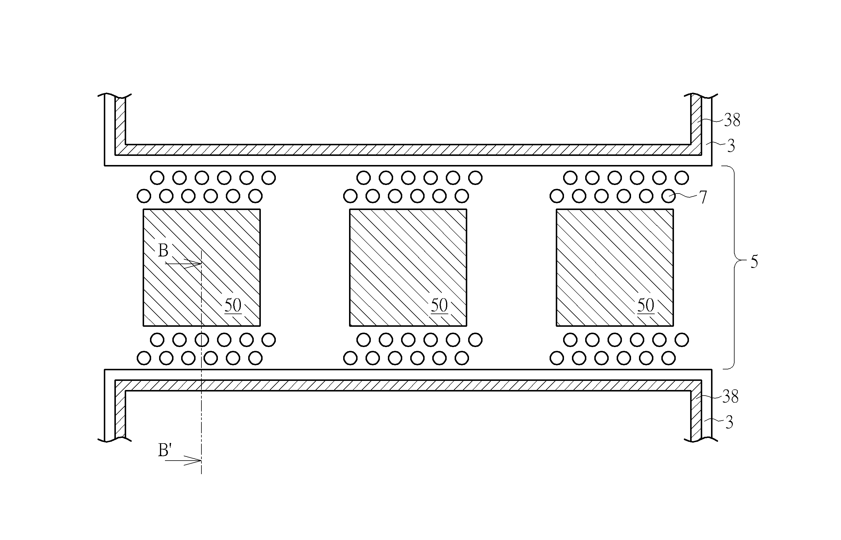
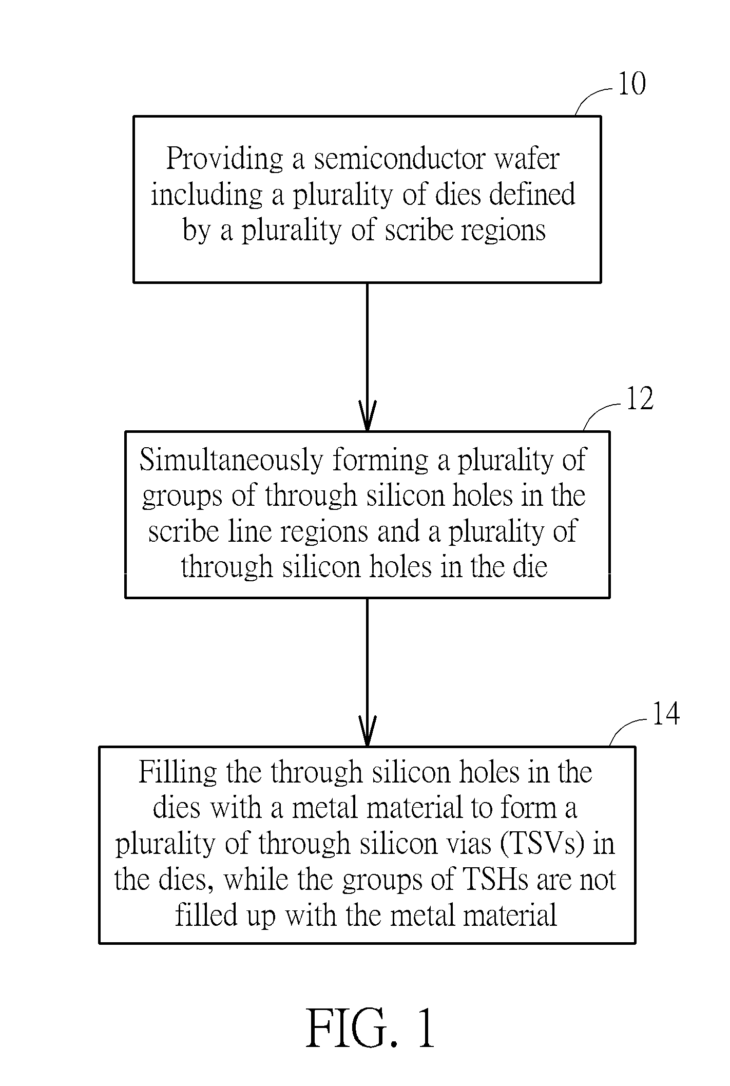
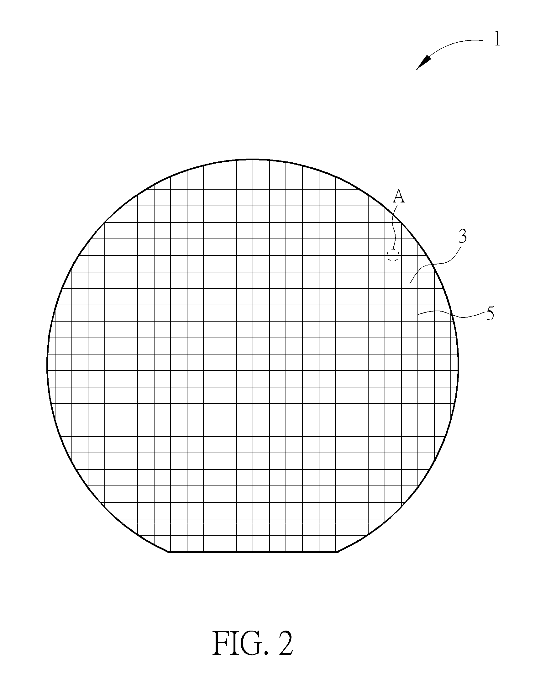
[0022]Please refer to FIGS. 1-7. FIG. 1 is a flow chart illustrating a method for forming a crack-stopping structure provided by a first preferred embodiment of the present invention. FIGS. 2-7 are schematic drawings illustrating a method for forming a crack-stopping structure provided by the first preferred embodiment, wherein FIG. 2 is a plan view showing an overall configuration of a semiconductor wafer, FIG. 3 is a partially enlarged view of Circle A of FIG. 2, FIG. 4 is a cross-sectional view taken along a Line B-B′ of FIG. 3, FIG. 5 is a partially enlarged view of Circle A of FIG. 2 and in a step subsequent to FIG. 3, and FIGS. 6-7 are cross-sectional views taken along a Line B-B′ of FIG. 5. As shown in FIG. 1, the method for forming a crack-stopping structure first provides a Step 10:

STEP 10: Providing a Semiconductor Wafer Comprising a Plurality of Dies Defined by a Plurality of Scribe Line Regions.

[0023]In order to clearly describe the structure of the present invention, FI...


PUM

PropertyMeasurementUnit
yieldaaaaaaaaaa
diameteraaaaaaaaaa
widthaaaaaaaaaa

Abstract

A crack-stopping structure includes a semiconductor wafer comprising a plurality of dies defined by a plurality of scribe line regions, a plurality of metal patterns formed in the scribe line regions, and a plurality of groups of through silicon holes (TSHs) formed in the scribe line regions. The wafer further includes a front side and a back side, and the TSHs respectively include at least a bottom opening formed in the bottom side of the wafer. The groups of TSHs are formed between the metal patterns and the dies.

Description

CROSS REFERENCE TO RELATED APPLICATIONS[0001]This application is a divisional of U.S. application Ser. No. 14 / 220,140, filed 20 Mar. 2014, the disclosure of which is hereby incorporated herein by reference in its entirety.BACKGROUND OF THE INVENTION[0002]1. Field of the Invention[0003]The invention relates to a crack-stopping structure and method for forming the same, and more particularly, to a wafer crack-stopping hollow structure and method for forming the same.[0004]2. Description of the Prior Art[0005]In the field of semiconductor device fabrication, semiconductor devices and interconnections are formed to construct integrated circuits (ICs) on a semiconductor wafer. The fabrication of ICs may be completed through different methods and steps, but generally involves depositing layers of conductive, semiconductor, and insulating materials in precise patterns on a substrate or wafer to form the desired circuit or array patterns. Once formed, the ICs then need to be separated into ...

Claims


Application Information

Patent Timeline
Patent Type & Authority Applications(United States)
IPC IPC(8): H01L23/544H01L21/56H01L23/00H01L21/768
CPCH01L23/544H01L21/76898H01L21/56H01L2223/54426H01L2223/5446H01L21/78H01L23/562H01L23/522H01L2223/5442H01L22/34H01L23/585H01L2924/37001H01L2924/14H01L2924/3512H01L2924/35121H01L2924/0002H01L23/481H01L2924/00H01L21/76232H01L21/784
Inventor TANG, KUANG-HUI
Owner UNITED MICROELECTRONICS CORP
Why Eureka
Try Eureka