High quality group-iii metal nitride seed crystal and method of making

a technology of metal nitride and seed crystal, which is applied in the direction of crystal growth process, polycrystalline material growth, after-treatment details, etc., can solve the problems of thermal expansion mismatch, impurities, tilt boundaries, and additional defects, etc., to achieve the effect of subsequently grown epitaxial layers, defects can be removed, and the quality and reliability of these devices are compromised

Active Publication Date: 2021-07-22
SLT TECH
View PDF3 Cites 1 Cited by
  • Summary
  • Abstract
  • Description
  • Claims
  • Application Information

AI Technical Summary

Benefits of technology

[0010]Embodiments of the disclosure may further include a method for forming a free-standing group III metal nitride crystal, comprising coupling a handle substrate to a template, wherein the template comprises a template substrate and a group III metal nitride layer, wherein the group III metal nitride layer is disposed over a first surface of the template substrate, and the handle substrate is polycrystalline and has a coefficient of thermal expansion in a first direction that is within ±15% of the group III metal nitride layer between room temperature and about 700 degrees Celsius and comprises substantially the same composition as the group III metal nitride laye...

Problems solved by technology

The quality and reliability of these devices, however, is compromised by high defect levels, particularly threading dislocations, grain boundaries, and strain in semiconductor layers of the devices.
Additional defects can arise from thermal expansion mismatch, impurities, and tilt boundaries, depending on the details of the growth of the layers.
The presence of defects has a deleterious effect on subsequently grown epitaxial layers.
Such effect includes compromising electronic device performance.
To overcome these defects, techniques have been proposed that require complex, tedious fabrication processes to reduce the concentration and/or impact of the defects.
While a substantial number of conventional growth methods for gallium nitride crystals have been proposed, limitations still exist.
Bow, stress, and strain can cause low yields when slicing the boules into wafers, make the wafers susceptible to cracking during down-stream processing, and may also negatively impact device reliability and lifetime.
For example, variable uptake of indium causes variatio...

Method used


Image

  • High quality group-iii metal nitride seed crystal and method of making
  • High quality group-iii metal nitride seed crystal and method of making
  • High quality group-iii metal nitride seed crystal and method of making

Examples


Embodiment Construction

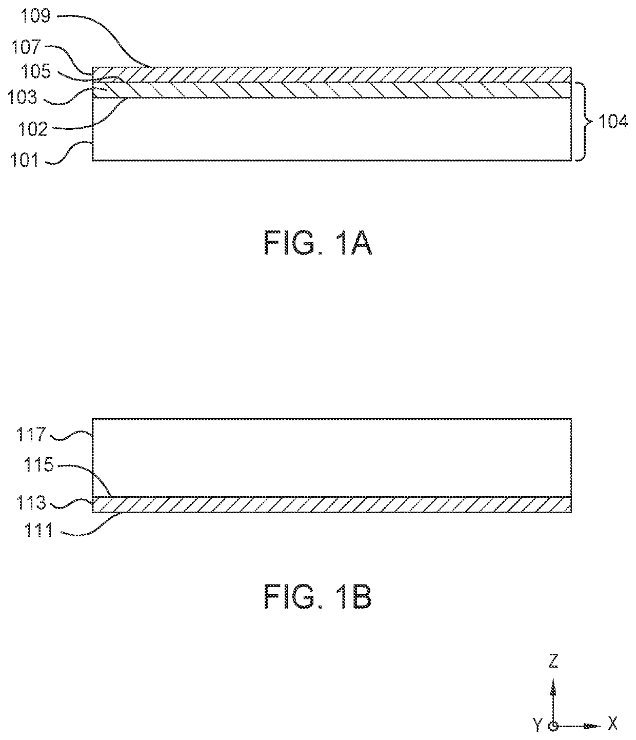
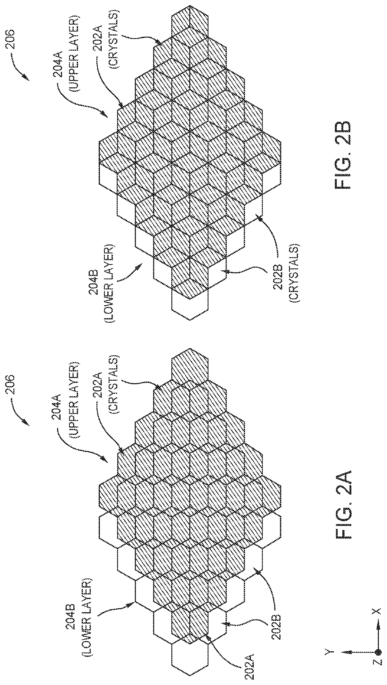
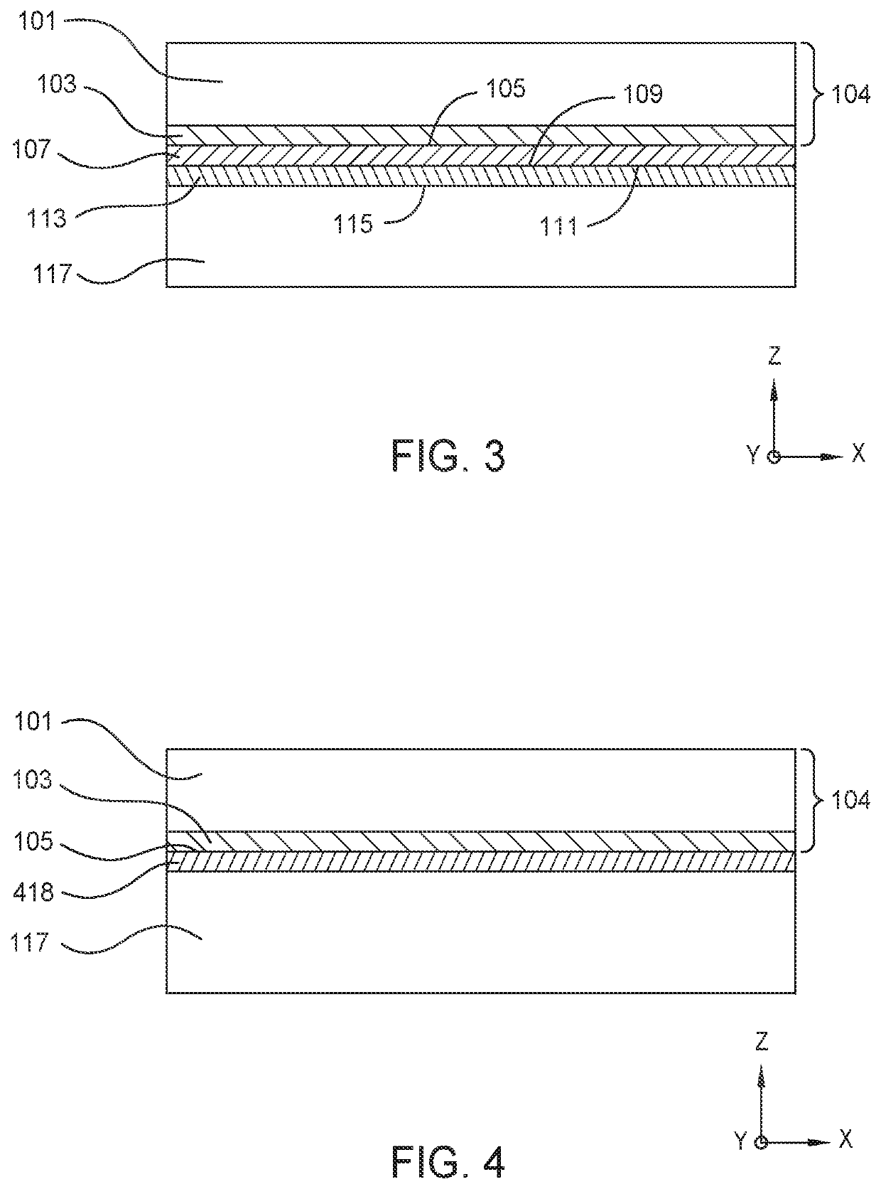
[0032]According to the present disclosure, techniques related to techniques for processing materials for manufacture of group-III metal nitride and gallium based substrates are provided. More specifically, embodiments of the disclosure include techniques for growing large area substrates using a combination of processing techniques. Merely by way of example, the disclosure can be applied to growing crystals of GaN, AlN, InN, InGaN, AlGaN, and AlInGaN, and others for manufacture of bulk or patterned substrates. Such bulk or patterned substrates can be used for a variety of applications including optoelectronic devices, lasers, light emitting diodes, solar cells, photo electrochemical water splitting and hydrogen generation, photodetectors, integrated circuits, and transistors, and others.

[0033]Threading dislocations in GaN are known to act as strong non-radiative recombination centers which can severely limit the efficiency of GaN-based LEDs and laser diodes. Non-radiative recombinat...


PUM


Abstract

High quality ammonothermal group III metal nitride crystals having a pattern of locally-approximately-linear arrays of threading dislocations, methods of manufacturing high quality ammonothermal group III metal nitride crystals, and methods of using such crystals are disclosed. The crystals are useful for seed bulk crystal growth and as substrates for light emitting diodes, laser diodes, transistors, photodetectors, solar cells, and for photoelectrochemical water splitting for hydrogen generation devices.

Description

CROSS-REFERENCE TO RELATED APPLICATIONS[0001]This application claims the benefit to U.S. Provisional Application No. 62 / 962,087, filed Jan. 16, 2020, which is incorporated by reference herein.BACKGROUNDField[0002]This disclosure relates generally to techniques for processing materials for manufacture of group-III metal nitride substrates, including gallium-containing nitride substrates. More specifically, embodiments of the disclosure include techniques for growing large area substrates using a combination of processing techniques. The disclosure can be applied to growing crystals of GaN, AlN, InN, InGaN, AlGaN, and AlInGaN, and others for manufacture of bulk or patterned substrates. Such bulk or patterned substrates can be used for a variety of applications including optoelectronic devices, lasers, light emitting diodes, solar cells, photo electrochemical water splitting, hydrogen generation, photo detectors, integrated circuits, power diodes, transistors, and others.Description of...

Claims


Application Information

Patent Timeline
IPC IPC(8): C30B7/10C30B29/40C30B28/04
CPCC30B7/105C30B28/04C30B29/406C30B29/403C30B33/00C30B33/06H01L33/007C30B25/04
Inventor D'EVELYN, MARK P.CARDWELL, DREW W.COOK, JONATHAN D.
Owner SLT TECH
Why Eureka
Try Eureka