Improved group iii nitride substrate, method of making, and method of use

a technology of nitride substrate and nitride, which is applied in the direction of polycrystalline material growth, crystal growth process, after-treatment details, etc., can solve the problems of thermal expansion mismatch, impurities, tilt boundaries, and additional defects that can arise from thermal expansion mismatch, etc., to achieve the effect of reducing the number of defects, and reducing the quality of the devi

Active Publication Date: 2021-08-12
SLT TECH
View PDF1 Cites 3 Cited by
  • Summary
  • Abstract
  • Description
  • Claims
  • Application Information

AI Technical Summary

Benefits of technology

[0004]The presence of defects has deleterious effects on epitaxially-grown layers. Such effects include compromising electronic device performance. To overcome these defects, techniques have been proposed that require complex, tedious fabrication processes to reduce the concentration and / or impact of the defects. While a substantial number of conventional growth methods for gallium nitride crystals have been proposed, limitations still exist. That is, conventional methods still merit improvement to be cost effective and efficient.

Problems solved by technology

The quality and reliability of these devices, however, is compromised by high defect levels, particularly threading dislocations, grain boundaries, and strain in semiconductor layers of the devices.
Additional defects can arise from thermal expansion mismatch, impurities, and tilt boundaries, depending on the details of the growth of the layers.
The presence of defects has deleterious effects on epitaxially-grown layers.
Such effects include compromising electronic device performance.
To overcome these defects, techniques have been proposed that require complex, tedious fabrication processes to reduce the concentration and / or impact of the defects.
While a substantial number of conventional growth methods for gallium nitride crystals have been proposed, limitations still exist.
Bow, stress, and strain can cause low yields when slicing the boules into wafers, make the wafers susceptible to cracking during down-stream processing, and may also negatively impact device reliability and lifetime.
In addition, the quality of c-plane growth may be unsatisfactory, due to formation of cracks, multiple crystallographic domains, and the like.
Capability to manufacture substrates larger than 2 inches is currently very limited, as is capability to produce large-area GaN substrates with a nonpolar or semipolar crystallographic orientation.
Most large area substrates are manufactured by vapor-phase methods, such as hydride vapor phase epitaxy (HVPE), which are relatively expensive.
However, the performance of ammonothermal GaN crystal growth processing may be significantly dependent on the size and quality of seed crystals.
Seed crystals fabricated by HVPE may suffer from many of the limitations described above, and large area ammonothermally-grown crystals are not widely available.
However, to the best of our knowledge, analogous methods have not yet been disclosed for bulk growth of GaN, including ammonothermal growth, and the methods that have been disclosed for sidewall LEO of thin-film GaN are impractical for bulk GaN.

Method used


Image

  • Improved group iii nitride substrate, method of making, and method of use
  • Improved group iii nitride substrate, method of making, and method of use
  • Improved group iii nitride substrate, method of making, and method of use

Examples


example 1

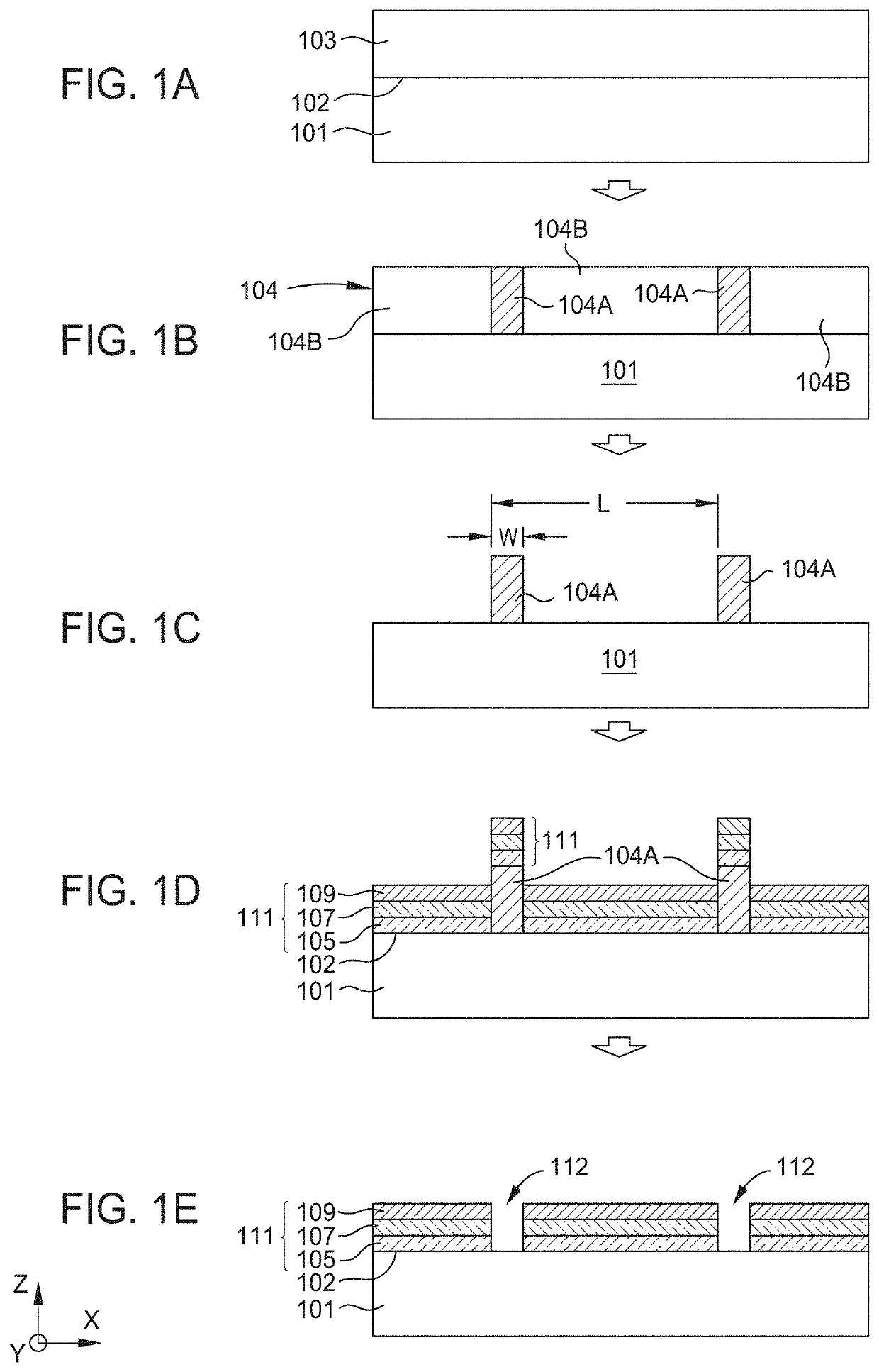
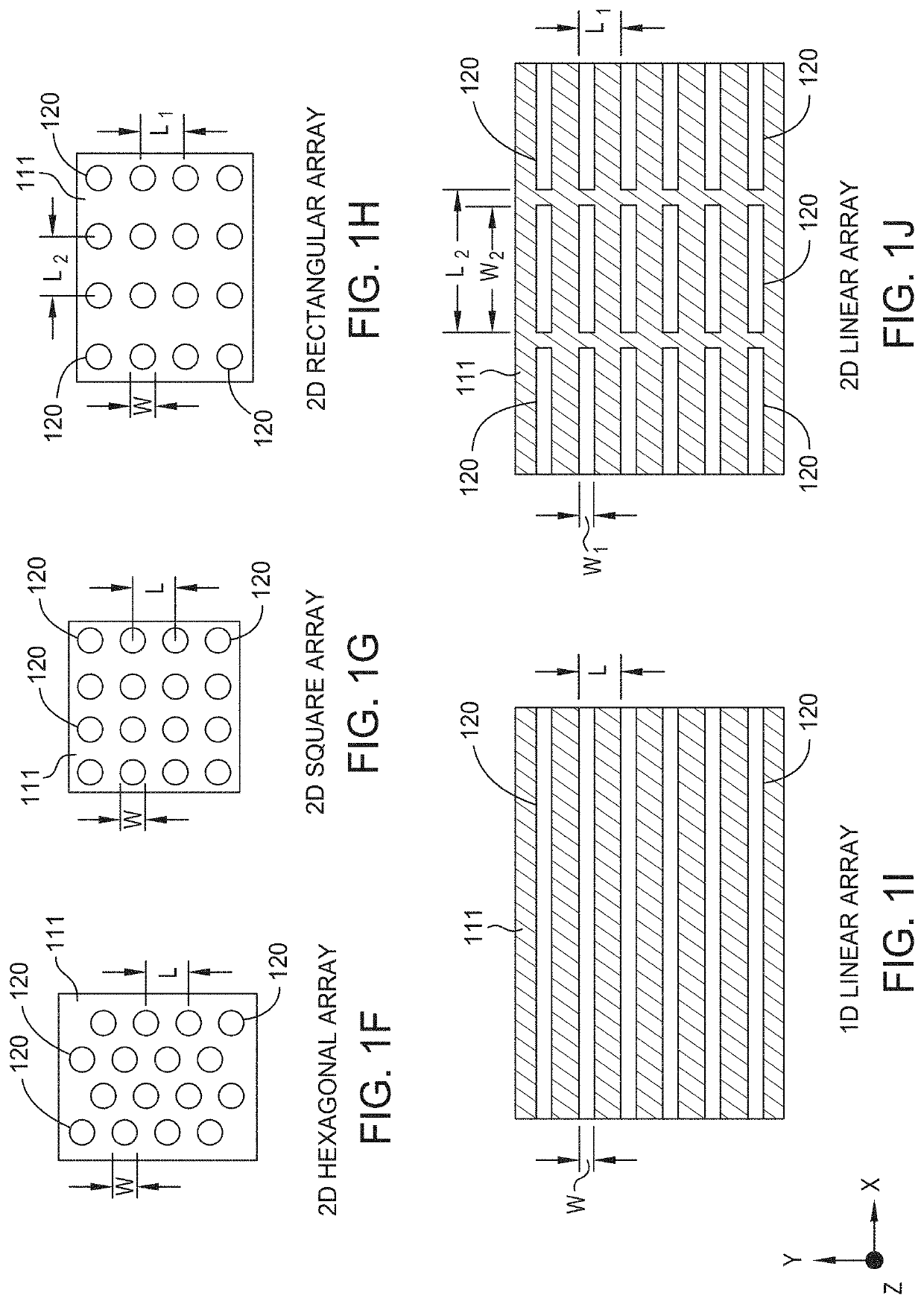
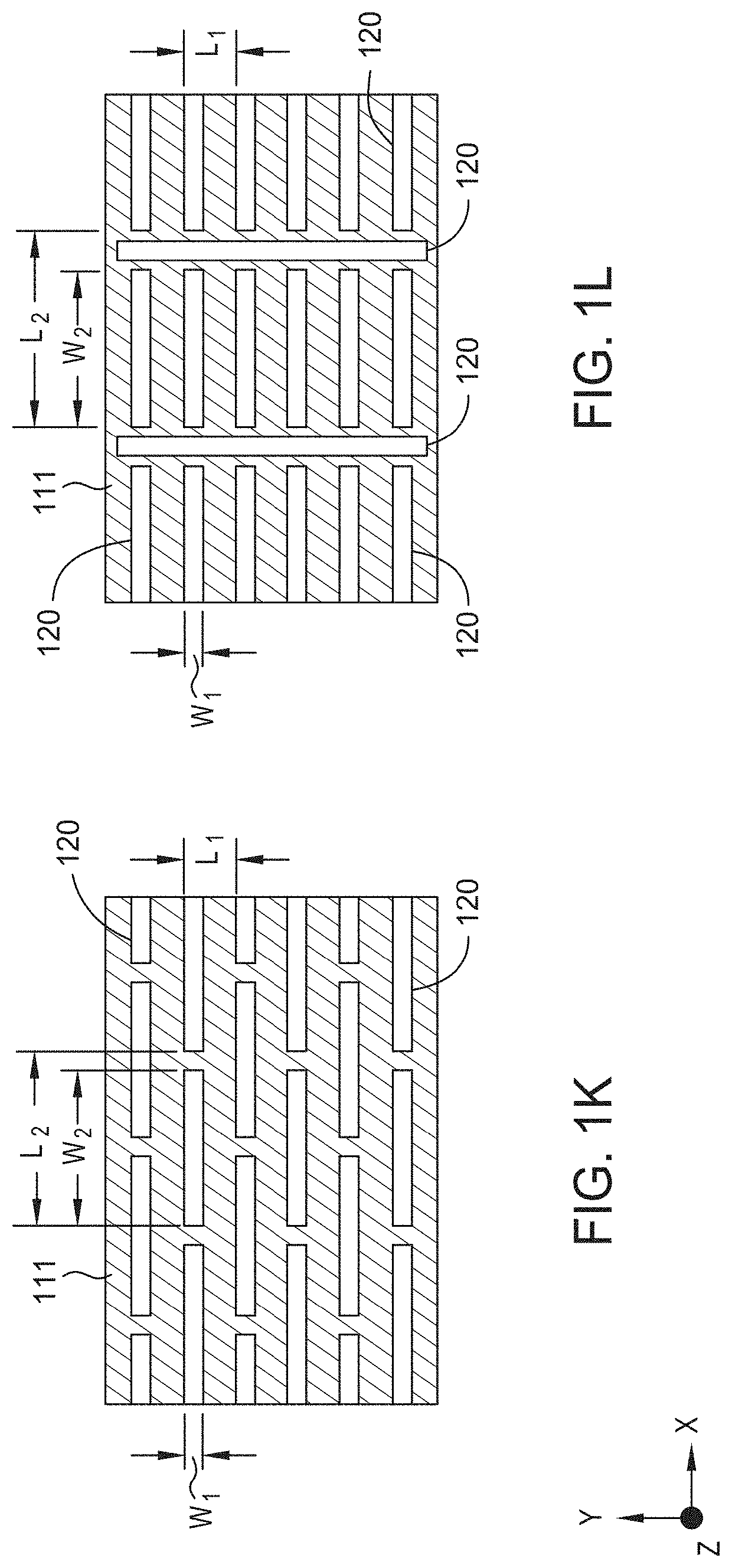
[0089]A c-plane oriented bulk GaN crystal grown by HVPE, approximately 0.3 millimeters thick, was provided for use as a substrate 101 for patterning and ammonothermal crystal growth. A 100-nanometer-thick layer of TiW was sputter-deposited as an adhesion layer on the (000-1) N-face of the substrate, followed by a 780-nanometer-thick inert layer comprising Au. A 6-micrometer-thick Au layer was then electroplated on the sputtered layer, increasing the thickness of the inert layer (e.g., blanket mask 116). Using AZ-4300 as a photoresist (e.g., photoresist layer 103), a pattern comprising linear arrays of 3-micrometer-wide by 1-centimeter-long slits (e.g., openings 112), with a pitch diameter of 1200 micrometers was defined. A wet-etch process was performed, using a commercial TFA gold etching solution at room temperature, as shown schematically in FIGS. 1M-1P, to obtain a substrate with patterned mask layer 111. The mask pattern comprised domains of m-stripes, with linear openings orie...

example 2

[0090]A patterned, trenched c-plane-oriented bulk GaN substrate 101 was prepared by a similar procedure as that described in Example 1. The patterned substrate was placed in a silver capsule along with a 15%-open-area baffle, polycrystalline GaN nutrient, NH4F mineralizer, and ammonia, and the capsule was sealed. The ratios of GaN nutrient and NH4F mineralizer to ammonia were approximately 1.69 and 0.099 respectively, by weight. The capsule was placed in an internally-heated high pressure apparatus and heated to temperatures of approximately 666 degrees Celsius for the upper, nutrient zone and approximately 681 degrees Celsius for the lower, crystal growth zone, maintained at these temperatures for approximately 215 hours, and then cooled and removed. Ammonothermal GaN filled in most of the volume in the trenches, grew through the linear openings in the patterned mask on the HVPE GaN substrate, grew laterally, and coalesced fully, forming an ammonothermal GaN layer approximately 120...

example 3

[0091]A patterned, trenched c-plane-oriented bulk GaN substrate was prepared by a similar procedure as that described in Examples 1 and 2, and the final group III metal nitride layer 213 is shown in FIG. 12B (i.e., right side figures). A second patterned substrate was prepared by a similar procedure except that no trenches were prepared below the mask openings, and the final group III metal nitride layer is shown in FIG. 12A (i.e., left side figures). The patterned substrates were placed in a silver capsule along with a 15%-open-area baffle, polycrystalline GaN nutrient, NH4F mineralizer, and ammonia, and the capsule was sealed. The ratios of GaN nutrient and NH4F mineralizer to ammonia were approximately 2.05 and 0.099 respectively, by weight. The capsule was placed in an internally-heated high pressure apparatus and heated to temperatures of approximately 666 degrees Celsius for the upper, nutrient zone and approximately 678 degrees Celsius for the lower, crystal growth zone, main...


PUM

PropertyMeasurementUnit
miscut angleaaaaaaaaaa
heightaaaaaaaaaa
thicknessaaaaaaaaaa

Abstract

Embodiments of the present disclosure include techniques related to techniques for processing materials for manufacture of group-III metal nitride and gallium based substrates. More specifically, embodiments of the disclosure include techniques for growing large area substrates using a combination of processing techniques. Merely by way of example, the disclosure can be applied to growing crystals of GaN, AlN, InN, InGaN, AlGaN, and AlInGaN, and others for manufacture of bulk or patterned substrates. Such bulk or patterned substrates can be used for a variety of applications including optoelectronic and electronic devices, lasers, light emitting diodes, solar cells, photo electrochemical water splitting and hydrogen generation, photodetectors, integrated circuits, and transistors, and others.

Description

CROSS-REFERENCE TO RELATED APPLICATIONS[0001]This application claims the benefit to U.S. provisional application No. 62 / 975,078, filed Feb. 11, 2020, which is incorporated by reference herein.BACKGROUNDField[0002]This disclosure relates generally to techniques for processing materials for manufacture of gallium-containing nitride substrates and utilization of these substrates in optoelectronic and electronic devices. More specifically, embodiments of the disclosure include techniques for growing large area substrates using a combination of processing techniques.Description of the Related Art[0003]Gallium nitride (GaN) based optoelectronic and electronic devices are of tremendous commercial importance. The quality and reliability of these devices, however, is compromised by high defect levels, particularly threading dislocations, grain boundaries, and strain in semiconductor layers of the devices. Threading dislocations can arise from lattice mismatch of GaN based semiconductor layer...

Claims


Application Information

Patent Timeline
Patent Type & Authority Applications(United States)
IPC IPC(8): H01L21/02C30B7/10C30B29/40C30B33/10C30B7/00
CPCH01L21/02005H01L21/02647H01L21/02642H01L21/0254H01L33/32C30B29/406C30B33/10C30B7/005C30B7/105H01L21/02389H01L21/02433H01L21/0262H01L29/861H01L29/8613H01L29/7788H01L29/2003H01L29/0646H01L33/007H01L21/0243
Inventor JIANG, WENKAND'EVELYN, MARK P.KAMBER, DERRICK S.EHRENTRAUT, DIRKCOOK, JONATHAN D.WENGER, JAMES
Owner SLT TECH
Why Eureka
Try Eureka