Light-activated semiconductor switches

a technology of light-activated semiconductors and switches, which is applied in the direction of instruments, optical elements, optics, etc., can solve the problems of reducing the voltage holding capacity of the device and compromising its electrical performance, so as to and reduce the voltage holding capacity

Active Publication Date: 2006-06-06
GENERAL ATOMICS
View PDF34 Cites 8 Cited by
  • Summary
  • Abstract
  • Description
  • Claims
  • Application Information

AI Technical Summary

Benefits of technology

[0008]Forming a groove deep into the semiconductor material of the switch, however, may result in the reduction of the voltage holding of the device, thus compromising its electrical performance. There is a need, therefore, for an approach that permits light activation of the switch, in which the light is able to reach the region over which the voltage is held, without reducing the voltage holding capabilities.
[0009]Accordingly, one aspect of the invention is directed to the use of sloped surfaces in the grooves that receive the optical fiber or the light therefrom. The use of a sloped surface increases the length of the surface path between points of different electrical potential in the groove, thus reducing the electric field along the groove and, therefore, permits the thyristor to operate closer to its theoretical breakdown voltage.

Problems solved by technology

Forming a groove deep into the semiconductor material of the switch, however, may result in the reduction of the voltage holding of the device, thus compromising its electrical performance.

Method used


Image

  • Light-activated semiconductor switches
  • Light-activated semiconductor switches
  • Light-activated semiconductor switches

Examples


Embodiment Construction

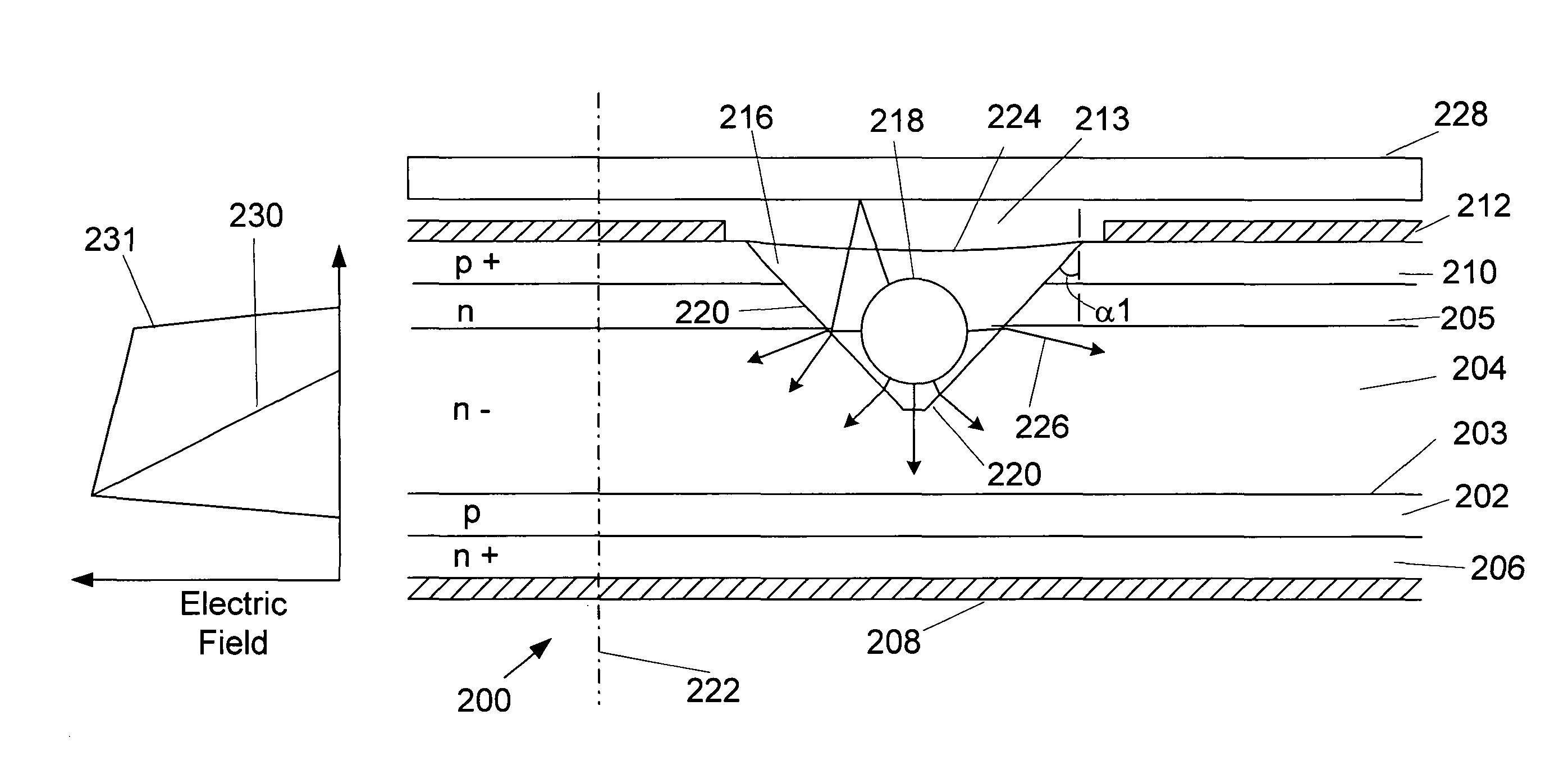
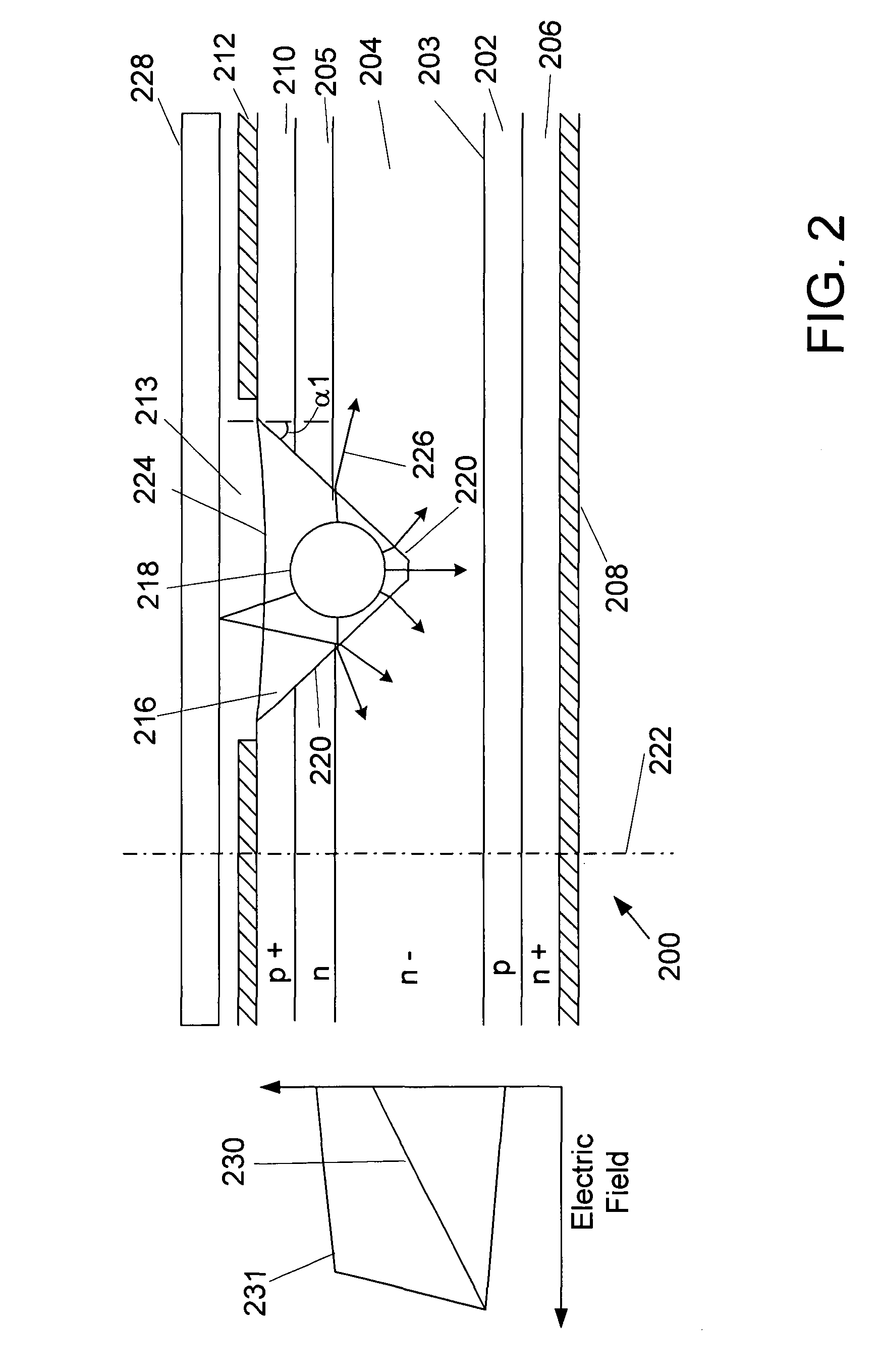
[0031]In general, the present invention is directed to light-activated semiconductor switches, and more particularly to an approach to activating a semiconductor switch using light that permits fast turn on to high current levels, while at the same time maintaining high voltage hold off.

[0032]The semiconductor devices described here are based on the use of optical triggering to actively switch the semiconductor switch into a conducting state. Optical activation involves illuminating the semiconductor switch with light. The light is absorbed within the semiconductor switch, resulting in the production of electron-hole pairs at the site of absorption. Thus, optical activation permits the direct generation of carrier pairs within the device, and does not require the injection of carriers into the device. Hence, optical activation can create carriers within the device considerably faster than injection, which process is limited in speed by the carrier drift velocity. Optical activation ...


PUM


Abstract

Semiconductor switches, such as thyristors, may be light activated by introducing the light into the switch via a groove having a sloped surface to receive the triggering light. The use of a sloped surface increases the surface path length between points of different electrical potential in the groove and, therefore, reduces the likelihood of electrical breakdown on the groove wall. In one particular embodiment, a light-activated thyristor includes a semiconductor anode layer, an n-base layer, a p-base layer and a semiconductor cathode layer disposed parallel to a thyristor plane. A thyristor axis lies perpendicular to the thyristor plane. A groove having a light refracting side wall extends into the thyristor from the anode layer. A portion of the light refracting side wall is disposed non-parallel to the thyristor plane and to the thyristor axis, and extends in the n-drift layer.

Description

FIELD OF THE INVENTION[0001]The present invention is directed generally to high power semiconductor devices and more particularly to a semiconductor switch that is activated by light.BACKGROUND[0002]The thyristor is a high power semiconductor switch that permits large currents to be switched at high voltages. The thyristor has four semiconducting layers. Typically, the two outer layers are heavily doped layers, while the inner two are lightly doped. Adjacent layers are oppositely doped from their neighbors, forming a number of semiconductor junctions therebetween.[0003]The thyristor is turned on when carriers enter one of the inner layers. Typically, this is performed by injecting a small gate current pulse into one of the inner layers. Where the gate current is injected over only a portion of the inner layer, the current through the thyristor does not reach a maximum value until the entire layer is conducting. The time taken for the current to spread laterally to fill the layer is ...

Claims


Application Information

Patent Timeline
Patent Type & Authority Patents(United States)
IPC IPC(8): H01L29/417H01L29/74H01L31/111G02B6/42
CPCG02B6/4204Y10S257/918
Inventor GIORGI, DAVID M.NAVAPANICH, TAJCHAI
Owner GENERAL ATOMICS
Why Eureka
Try Eureka