Liquid crystal display pixel structure and manufacture method thereof

a liquid crystal display and pixel technology, applied in non-linear optics, instruments, optics, etc., can solve the problems of reducing the pixel aperture ratio, the control circuit is more complicated, and the effect is not well, so as to simplify the driving control circuit, improve the color washout phenomenon, and reduce the number of tfts

Active Publication Date: 2016-11-24
SHENZHEN CHINA STAR OPTOELECTRONICS TECH CO LTD
View PDF6 Cites 4 Cited by
  • Summary
  • Abstract
  • Description
  • Claims
  • Application Information

AI Technical Summary

Benefits of technology

[0029]The benefits of the present invention are: the present invention provides a liquid crystal display pixel structure, by locating at least two trench structures having different depths to the passivation layer in one pixel for dividing the one pixel into different areas, realizes that liquid crystals in different areas of the one pixel have different twisted angles under the same driving voltage, which can significantly improve the color washout phenomenon under wide view angle. Compared with the liquid crystal display pixel structure according to prior art, the number of the TFTs can be diminished to simplify the driving control circuit and raise the pixel aperture ratio; the present invention provides a manufacture method of the liquid crystal display pixel structure, by etching the passivation layer in one pixel to comprise at least two trench structures having different depths and directly deposing the pixel electrode on the trench structures, so that the high transmission ratio can be achieved without the high accuracy trench structures. The demands to photo apparatus and manufacture process are lower. The color washout phenomenon of the liquid crystal display pixel structure obtained by the manufacture method under wide view angle can be significantly improved.

Problems solved by technology

However, more TFTs mean more complicated control circuit and descend of the pixel aperture ratio.
Although each pixel comprises four domains and provides a certain improvement to the color washout under wide view angle, the effect is not well.
The color washout is still serious.

Method used


Image

  • Liquid crystal display pixel structure and manufacture method thereof
  • Liquid crystal display pixel structure and manufacture method thereof
  • Liquid crystal display pixel structure and manufacture method thereof

Examples


Embodiment Construction

[0046]For better explaining the technical solution and the effect of the present invention, the present invention will be further described in detail with the accompanying drawings and the specific embodiments.

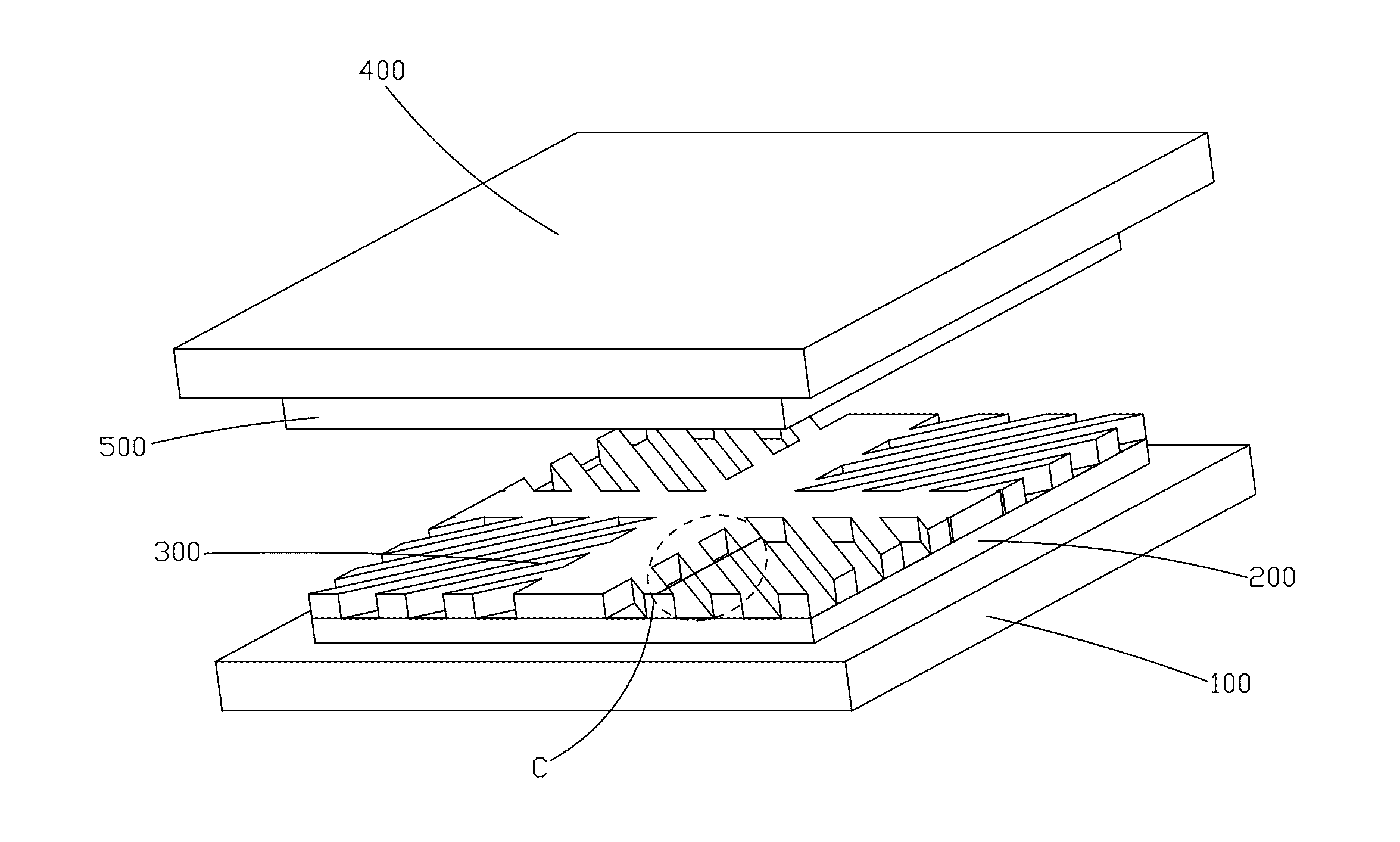
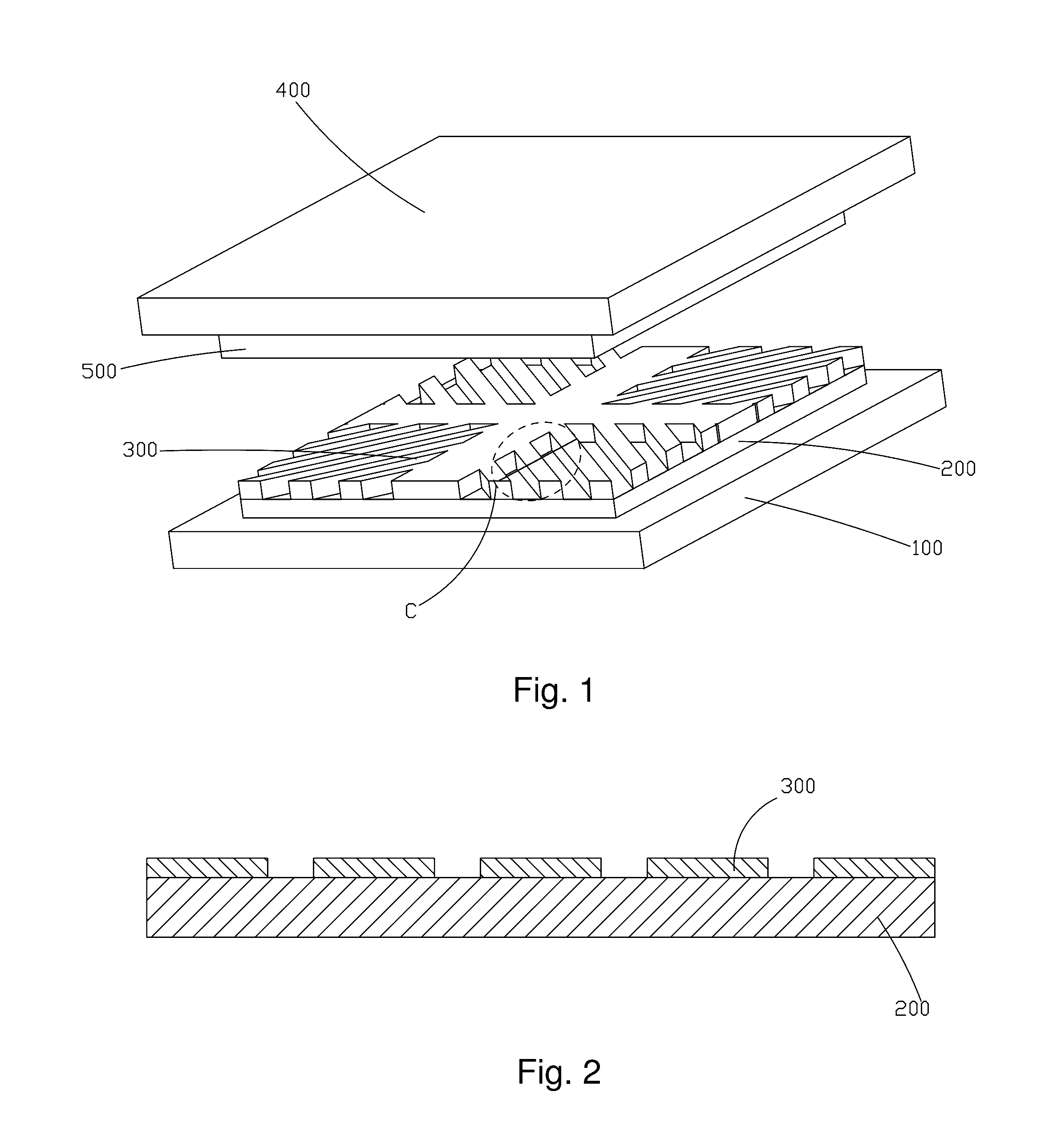
[0047]Please refer to FIG. 6, FIG. 7, FIG. 8, which show a liquid crystal display pixel structure according to the first embodiment of the present invention at the same time. It comprises: a lower substrate 1, a passivation layer 2 located on an upper surface of the lower substrate 1, a pixel electrode 3 located on the passivation layer 2, an upper substrate 4 and a common electrode 5 located on a lower surface of the upper substrate 4.

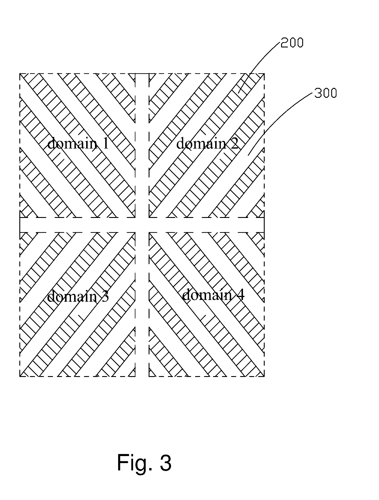
[0048]The pixel electrode 3 is an ITO electrode, and the common electrode 5 is an ITO electrode. Each pixel comprises multi domains; in one pixel, the passivation layer 2 comprises at least two trench structures having different depths, and the pixel electrode 3 uninterruptedly covers on the trench structures, the trench structures having differ...


PUM

PropertyMeasurementUnit
depthsaaaaaaaaaa
thicknessaaaaaaaaaa
widthaaaaaaaaaa

Abstract

The present invention provides a liquid crystal display pixel structure and a manufacture method thereof. The liquid crystal display pixel structure comprises: a lower substrate (1), a passivation layer (2) located on an upper surface of the lower substrate (1), a pixel electrode (3) located on the passivation layer (2), an upper substrate (4), and a common electrode (5) located on a lower surface of the upper substrate (4); each pixel comprises multi domains; in one pixel, the passivation layer (2) comprises at least two trench structures having different depths, and the pixel electrode uninterruptedly covers on the trench structures, the trench structures having different depths divide the one pixel into different areas to realize that liquid crystals in different areas of the one pixel have different twisted angles under the same driving voltage. The liquid crystal display pixel structure of the present invention is capable of improving the color washout phenomenon under wide view angle, and simplifying the driving control circuit and raising the pixel aperture ratio.

Description

FIELD OF THE INVENTION[0001]The present invention relates to a display technology field, and more particularly to a liquid crystal display pixel structure and manufacture method thereof.BACKGROUND OF THE INVENTION[0002]The LCD (Liquid Crystal Display) possesses advantages of thin body, power saving and no radiation to be widely used in many application scope, such as LCD TV, mobile phone, personal digital assistant (PDA), digital camera, notebook, laptop, and dominates the flat panel display field.[0003]Most of the liquid crystal displays on the present market are back light type liquid crystal displays, which comprise a shell, a liquid crystal display panel located in the shell and a backlight module located in the shell. The liquid crystal display panel is the major component of the liquid crystal display. However, the liquid crystal display panel itself does not emit light and needs the back light module to provide light source for normally showing images.[0004]Generally, the liq...

Claims


Application Information

Patent Timeline
Patent Type & Authority Applications(United States)
IPC IPC(8): G02F1/1343G02F1/1333G02F1/1337G02F1/1368
CPCG02F1/13439G02F1/1337G02F1/134309G02F2001/133397G02F1/133345G02F2201/123G02F2201/40G02F1/1368G02F2201/121G02F1/1333G02F1/136G02F1/136295G02F1/13378G02F1/133792G02F1/133397
Inventor ZHAO, FENGCHIU, CHUNGYI
Owner SHENZHEN CHINA STAR OPTOELECTRONICS TECH CO LTD
Why Eureka
Try Eureka