Package structure and method for manufacturing the same

Active Publication Date: 2016-11-24
UNIMICRON TECH CORP
View PDF5 Cites 7 Cited by
  • Summary
  • Abstract
  • Description
  • Claims
  • Application Information

AI Technical Summary

Benefits of technology

[0007]The invention is directed to a three-dimensional (3D) package structure and a method for manufacturing

Problems solved by technology

However, since the prepreg or the other suitable dielectric material is relatively soft, a warpage issue of the multi-layer circuit structure is probably encountered during the manufacturing

Method used


Image

  • Package structure and method for manufacturing the same
  • Package structure and method for manufacturing the same
  • Package structure and method for manufacturing the same

Examples


first embodiment

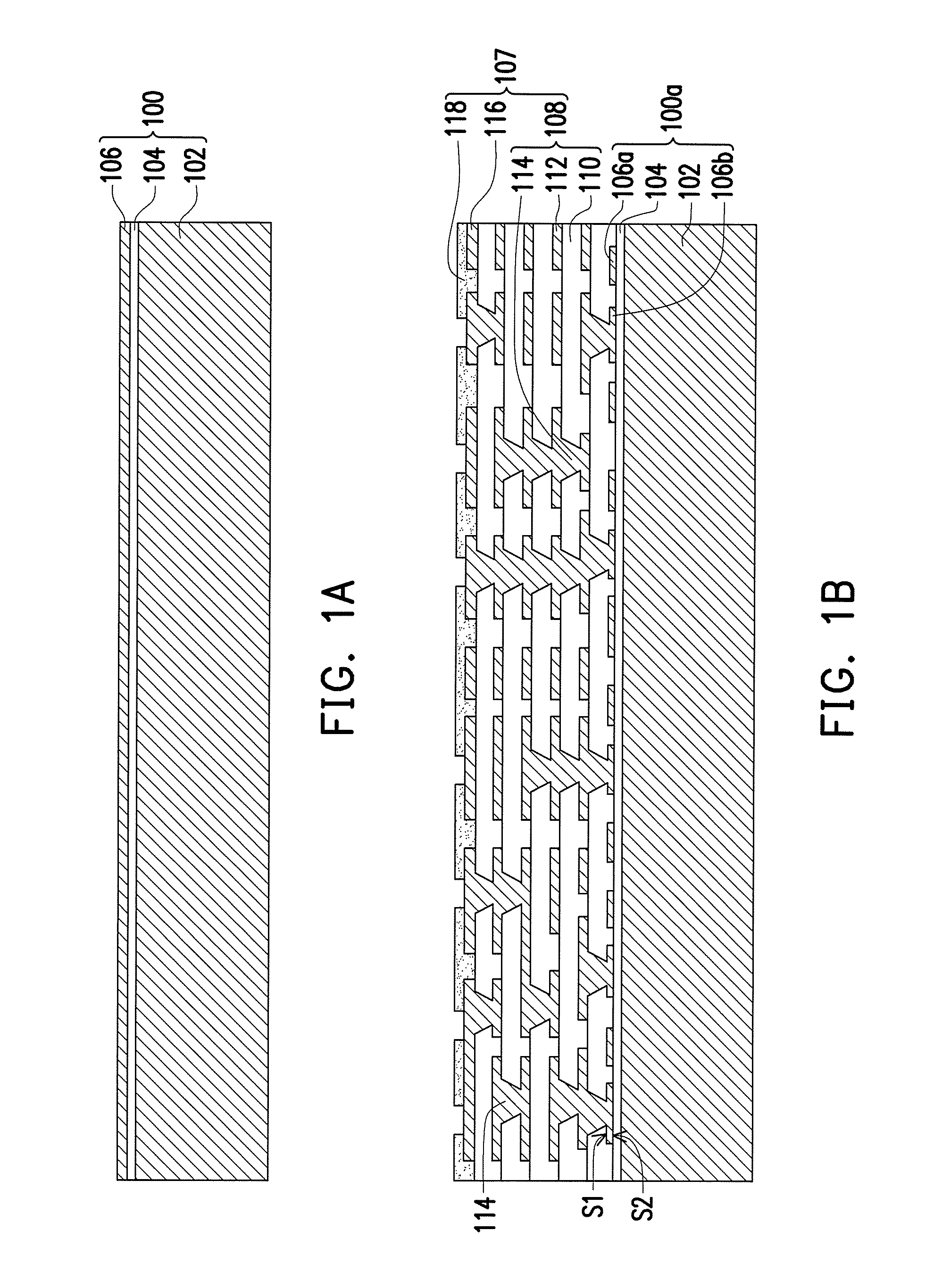
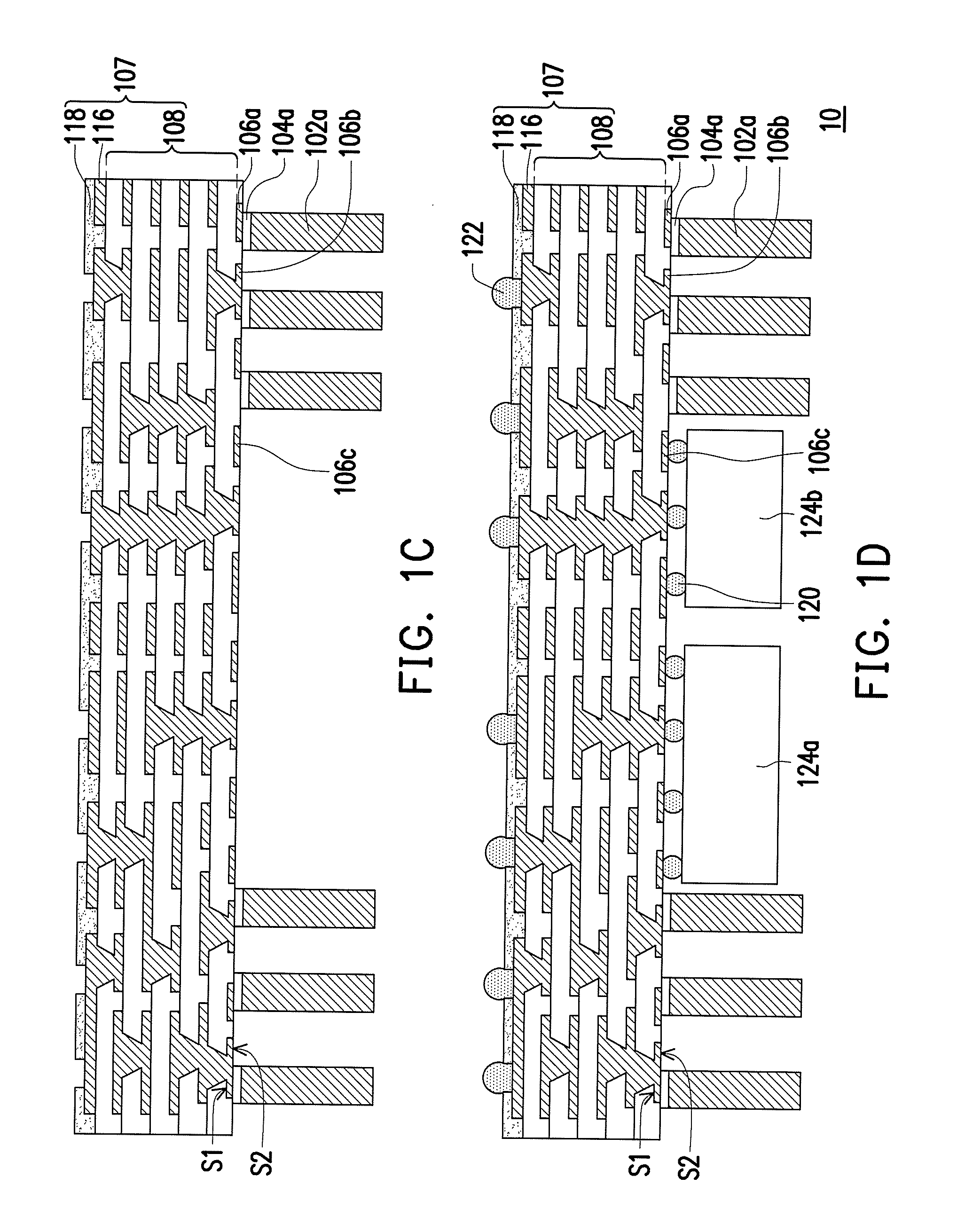
[0037]FIG. 1A to FIG. 1D are cross-sectional views of a manufacturing process of a package structure according to the invention.

[0038]Referring to FIG. 1A, a substrate 100 is provided. The substrate 100 includes a first metal layer 102, a second metal layer 106 and an etching stop layer 104. The etching stop layer 104 is disposed between the first metal layer 102 and the second metal layer 106. In the present embodiment, the substrate 100 is, for example, a three-layer structure composed of Cu—Ni—Cu, or a three-layer structure composed of Cu—Al—Cu, as long as a material of the etching stop layer 104 is different to the material of the first metal layer 102 and the material of the second metal layer 106, though the invention is not limited thereto. In other embodiment, the material of the first metal layer 102 is, for example, silver, nickel, copper, aluminium, gold, palladium or a combination thereof, and a thickness thereof is between 10 μm and 150 μm. The material of the second me...

second embodiment

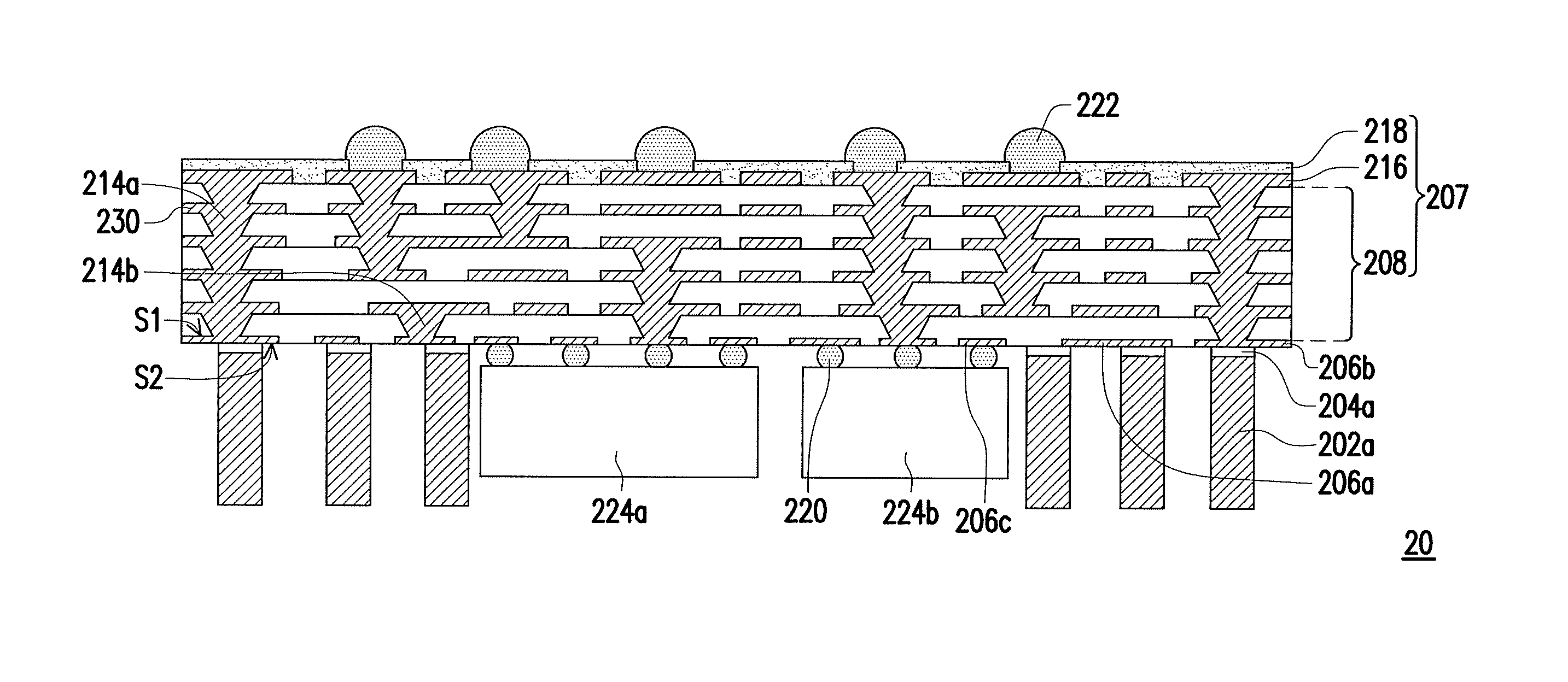
[0047]FIG. 2A to FIG. 2D are cross-sectional views of a manufacturing process of a package structure according to the invention. FIG. 3 is a top view of a supporting structure of FIG. 2B.

[0048]Referring to FIG. 2A to FIG. 2C, the manufacturing process of the package structure 20 of the second embodiment of the invention is basically similar to the manufacturing process of the package structure 10 of the first embodiment, and a difference therebetween is that besides the conductive through vias 214b (similar to the conductive through vias 114 of the first embodiment), the circuit board 207 of the second embodiment further has a plurality of conductive through vias 214a disposed in the dielectric layer 210. The conductive through vias 214a can be disposed around the circuit board 207 (regarding the cross-sectional view of FIG. 2B, the surrounding of the circuit board 207 can be regarded to be close to two sides 226 and 228 of the circuit board 207). The conductive through vias 214a ar...

third embodiment

[0051]FIG. 4A to FIG. 4D are cross-sectional views of a manufacturing process of a package structure according to the invention. FIG. 5 is a top view of a heat dissipation structure of FIG. 4A.

[0052]The manufacturing process of the package structure 30 of the third embodiment of the invention is basically similar to the manufacturing process of the package structure 20 of the second embodiment. Referring to FIG. 4A, FIG. 2B and FIG. 5, a difference between the embodiments of FIG. 4A and FIG. 2B is that the circuit board 307 of the third embodiment further has the first heat dissipation structure 330 and a dielectric layer 332 disposed between the build-up structure 308 and the second contact pads 316. As shown in FIG. 4A, the first heat dissipation structure 330 is electrically connected to the vertical supporting structure 314a (i.e., the conductive through vias 314a) to form an inverted U-shape structure. In detail, the first heat dissipation structure 330 can be regarded as anoth...


PUM


Abstract

Provided is a package structure including a circuit board, a plurality of first contact pads, a plurality of metal pillars and at least one chip. The first contact pads are disposed on the circuit board. The chip is disposed on one portion of the first contact pads. The metal pillars are disposed on the other portion of the first contact pads, where the chip is surrounded by the metal pillars. A method for manufacturing the package structure is also provided.

Description

CROSS-REFERENCE TO RELATED APPLICATION[0001]This application claims the priority benefit of Taiwan application serial no. 104116526, filed on May 22, 2015. The entirety of the above-mentioned patent application is hereby incorporated by reference herein and made a part of this specification.BACKGROUND OF THE INVENTION[0002]1. Field of the Invention[0003]The invention relates to a semiconductor structure and a method for manufacturing the same, and particularly relates to a three-dimensional package structure and a method for manufacturing the same.[0004]2. Description of Related Art[0005]In recent years, in order to increase applications of printed circuit board (PCB), the PCB is fabricated into a multi-layer circuit structure according to many techniques. A method for fabricating the multi-layer circuit structure is to construct a build-up structure by using copper foils or other suitable conductive materials and prepreg (PP) or other suitable dielectric materials, and repeatedly l...

Claims


Application Information

Patent Timeline
IPC IPC(8): H01L23/498H01L21/48H01L23/00
CPCH01L23/49811H01L21/481H01L24/81H01L23/49827H01L2924/37001H01L23/16H01L23/36H01L23/3735H01L23/49805H01L21/486H01L23/5383H01L23/562H01L24/16H01L24/73H01L25/0655H01L25/105H01L2224/16227H01L2224/16235H01L2224/73253H01L2225/1058H01L2924/15311H01L2924/1533H01L2924/18161H01L2924/3511H01L23/5384
Inventor PAN, PI-TECHEN, CHANG-FU
Owner UNIMICRON TECH CORP
Why Eureka
Try Eureka