Display device

a display module and touch panel technology, applied in the field of display devices, can solve the problems of increasing the number of components and the inability to reduce the thickness of the touch panel (or the display module), and achieve the effects of simple structure, increased thickness of the touch panel (or the display module), and reduced thickness

Active Publication Date: 2016-12-15
SEMICON ENERGY LAB CO LTD
View PDF0 Cites 21 Cited by
  • Summary
  • Abstract
  • Description
  • Claims
  • Application Information

AI Technical Summary

Benefits of technology

[0014]For example, in a touch panel (or a display module), a substrate provided with a touch sensor can be attached to the display surface side of a display panel. In other words, in a touch panel (or a display module), a display panel and a touch sensor can be separate components and can be attached to each other. However, in such a structure, a substrate for a touch sensor is needed in addition to a substrate for a display panel, resulting in that the thickness of a touch panel (or a display module) cannot be reduced and the number of components is increased.
[0015]An object of one embodiment of the present invention is to provide a thin touch panel (or a thin touch sensor equipped display device) and the like. Another object is to provide a touch panel (or a touch sensor equipped display device) with a simple structure and the like. Another object is to provide a touch panel (or a touch sensor equipped display device) which can be easily incorporated into an electronic device and the like. Another object is to provide a touch panel (or a touch sensor equipped display device) with a small number of components and the like. Another object is to provide a lightweight touch panel (or a lightweight touch sensor equipped display device) and the like.

Problems solved by technology

However, in such a structure, a substrate for a touch sensor is needed in addition to a substrate for a display panel, resulting in that the thickness of a touch panel (or a display module) cannot be reduced and the number of components is increased.

Method used


Image

  • Display device
  • Display device
  • Display device

Examples


embodiment 1

[0122]This embodiment describes driving methods, modes, structure examples of a touch sensor or a touch panel of one embodiment of the present invention and structure examples of a semiconductor device of one embodiment of the present invention with reference to drawings.

[Example of Sensing Method of Sensor]

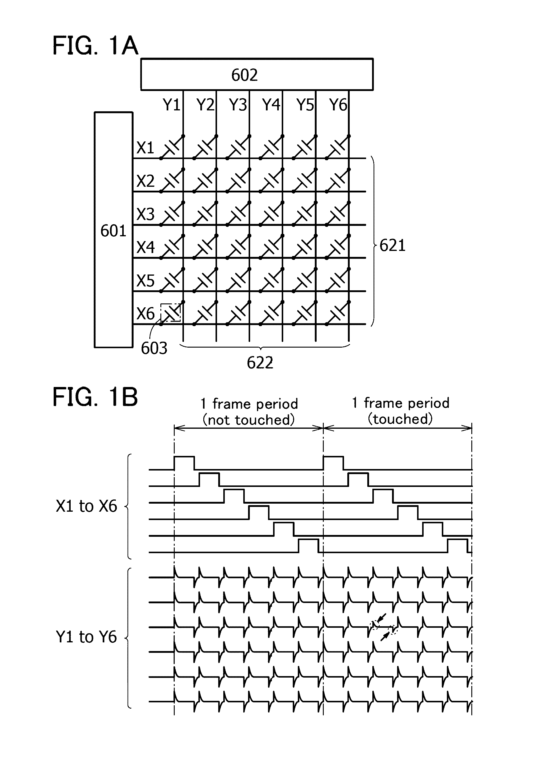
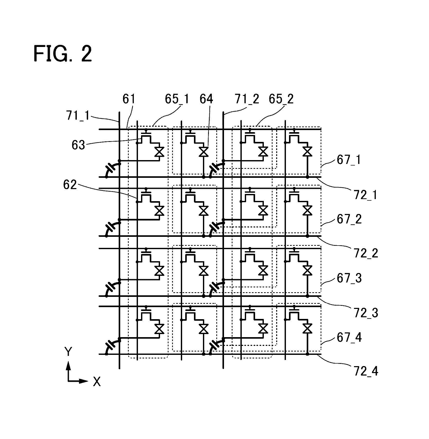
[0123]FIG. 1A is a block diagram illustrating structures of mutual capacitive touch sensors. FIG. 1A illustrates a pulse voltage output circuit 601 and a current sensing circuit 602. In FIG. 1A, as an example, six wirings X1 to X6 represent electrodes 621 to which a pulse voltage is applied, and six wirings Y1 to Y6 represent electrodes 622 that sense changes in current. The number of such electrodes is not limited to those illustrated in this example. FIG. 1A also illustrates capacitors 603 each of which is formed with the electrodes 621 and 622 overlapping with each other or being provided close to each other. Note that the functions of the electrodes 621 and 622 can be interch...

structure example 1

[0200]More specific structure examples of the display device or the touch panel are described below. Structure examples to be described below and the structure examples described above can be combined with or applied to each other. Therefore, in a structure example to be described below, part thereof can be modified into any of the structure examples described above.

[0201]FIG. 22A is an example of a schematic top view of a display device 310 of one embodiment of the present invention. Note that in FIG. 22A, only components provided on an element substrate side are illustrated and a counter substrate side is not illustrated. In addition, only main components are illustrated in FIG. 22A for simplicity.

[0202]The display device 310 includes a substrate 102 and a substrate 372 (not illustrated) which face each other.

[0203]A display portion 381, a wiring 382, a driver circuit 383, a driver circuit 384, a wiring 386, and the like are provided over the substrate 102 (see FIG. 22A). A conduc...

example 1

Cross-Sectional Structure Example 1

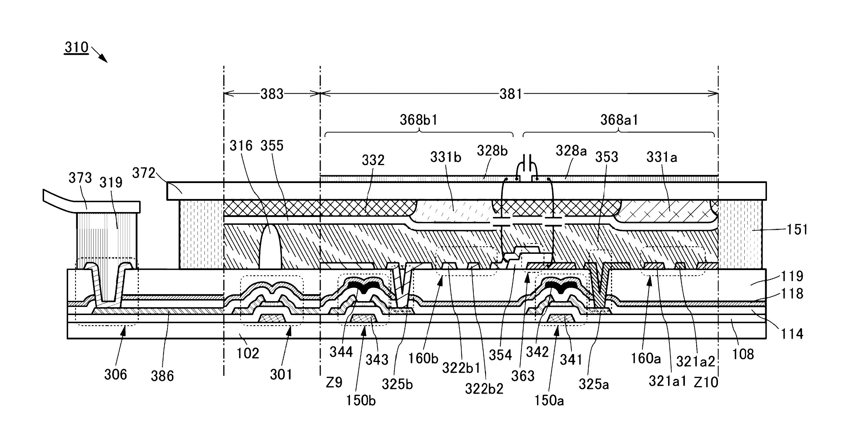
[0250]Examples of the cross-sectional structure of the display device of one embodiment of the present invention are described below with reference to drawings.

[0251]FIG. 42 is a schematic cross-sectional view of the display device 310. FIG. 42 illustrates the cross sections of a region including the FPC 373, a region including the driver circuit 383, and a region including the display portion 381 in FIG. 22A.

[0252]The substrate 102 and the substrate 372 are attached to each other with a sealant 151. A region surrounded by the substrate 102, the substrate 372, and the sealant 151 is filled with liquid crystal 353.

[0253]A transistor 301, a transistor 150a, a transistor 150b, the wiring 386, the conductive films 321a, 321b, 322a, and 322b included in liquid crystal elements 160a and 160b, and the like are provided over the substrate 102.

[0254]An insulating film 108, an insulating film 114, an insulating film 118, an insulating film 119, an insulating...


PUM


Abstract

A display device includes a first pixel, a second pixel, a first substrate, and a second substrate. The first pixel includes a first pixel electrode, a first conductive film, and a first transistor. The first pixel electrode is electrically connected to the first transistor. The first conductive film includes a region functioning as a common electrode. The second pixel includes a second pixel electrode, a second conductive film, and a second transistor. The second pixel electrode is electrically connected to the second transistor. The second conductive film includes a region functioning as a common electrode. The first conductive film and the second pixel electrode are provided on the same plane. A first insulating film is provided over the first conductive film and the second pixel electrode. The first pixel electrode and the second conductive film are provided over the first insulating film.

Description

BACKGROUND OF THE INVENTION[0001]1. Field of the Invention[0002]One embodiment of the present invention relates to a display device. One embodiment of the present invention relates to a touch panel. One embodiment of the present invention relates to a semiconductor device. One embodiment of the present invention relates to an input / output device. One embodiment of the present invention relates to an input device. One embodiment of the present invention relates to a display device with a built-in touch sensor.[0003]Note that one embodiment of the present invention is not limited to the above technical field. One embodiment of the invention disclosed in this specification and the like relates to an object, a method, or a manufacturing method. One embodiment of the present invention relates to a process, a machine, manufacture, or a composition of matter. Specifically, examples of the technical field of one embodiment of the present invention disclosed in this specification and the lik...

Claims


Application Information

Patent Timeline
Patent Type & Authority Applications(United States)
IPC IPC(8): H01L27/12G06F3/047G06F3/044G06F3/041
CPCH01L27/1225G06F3/044G06F3/047G06F3/0412G06F3/04166G06F3/0445G06F3/0446G06F3/0448G02F1/136227
Inventor KIMURA, HAJIMEKUBOTA, DAISUKEYAMAZAKI, SHUNPEI
Owner SEMICON ENERGY LAB CO LTD
Why Eureka
Try Eureka