Sensor chip for surface plasmon-field enhanced fluorescence spectroscopy

a technology of fluorescence spectroscopy and plasmon field, which is applied in the direction of fluorescence/phosphorescence, instruments, and material excitation, can solve the problems of reducing the detection efficiency of surface plasmons. the effect of inhibiting

Inactive Publication Date: 2016-12-22
KONICA MINOLTA INC
View PDF4 Cites 11 Cited by
  • Summary
  • Abstract
  • Description
  • Claims
  • Application Information

AI Technical Summary

Benefits of technology

[0026]According to the present invention, a sensor chip in which non-specific adsorption of contaminants originating from a measurement sample (biological sample) to a sensor section is effectively inhibited and the effect of blocking autofluorescence emitted by a dielectric member is not reduced with time is provided.

Problems solved by technology

Further, one of the causes of the baseline signal is autofluorescence generated by the material of the dielectric member such as a prism; however, since such autofluorescence is mostly blocked by the metal thin film, it does not reach the light-detecting means and the baseline signal is thus suppressed.
However, there are cases where the metal thin film is partially detached from a dielectric member with lapse of time.
That is, the metal thin film is usually formed on a main surface of the dielectric member by a plasma-assisted sputtering method, a vacuum film-forming method such as electron beam-heating vacuum vapor deposition, or the like; however, after the metal thin film is subjected to a blocking treatment as described above, a phenomenon that the metal thin film partially swells in a circular form and is detached from the dielectric member occurs with time in some cases.
It is now understood that, as a result of such phenomenon, the autofluorescence generated by the material of the dielectric member is no longer sufficiently blocked by the metal thin film, and this leads to an increase in the baseline signal and generation of noise.

Method used


Image

  • Sensor chip for surface plasmon-field enhanced fluorescence spectroscopy
  • Sensor chip for surface plasmon-field enhanced fluorescence spectroscopy
  • Sensor chip for surface plasmon-field enhanced fluorescence spectroscopy

Examples


example 1

(1) Preparation of Sensor Chip

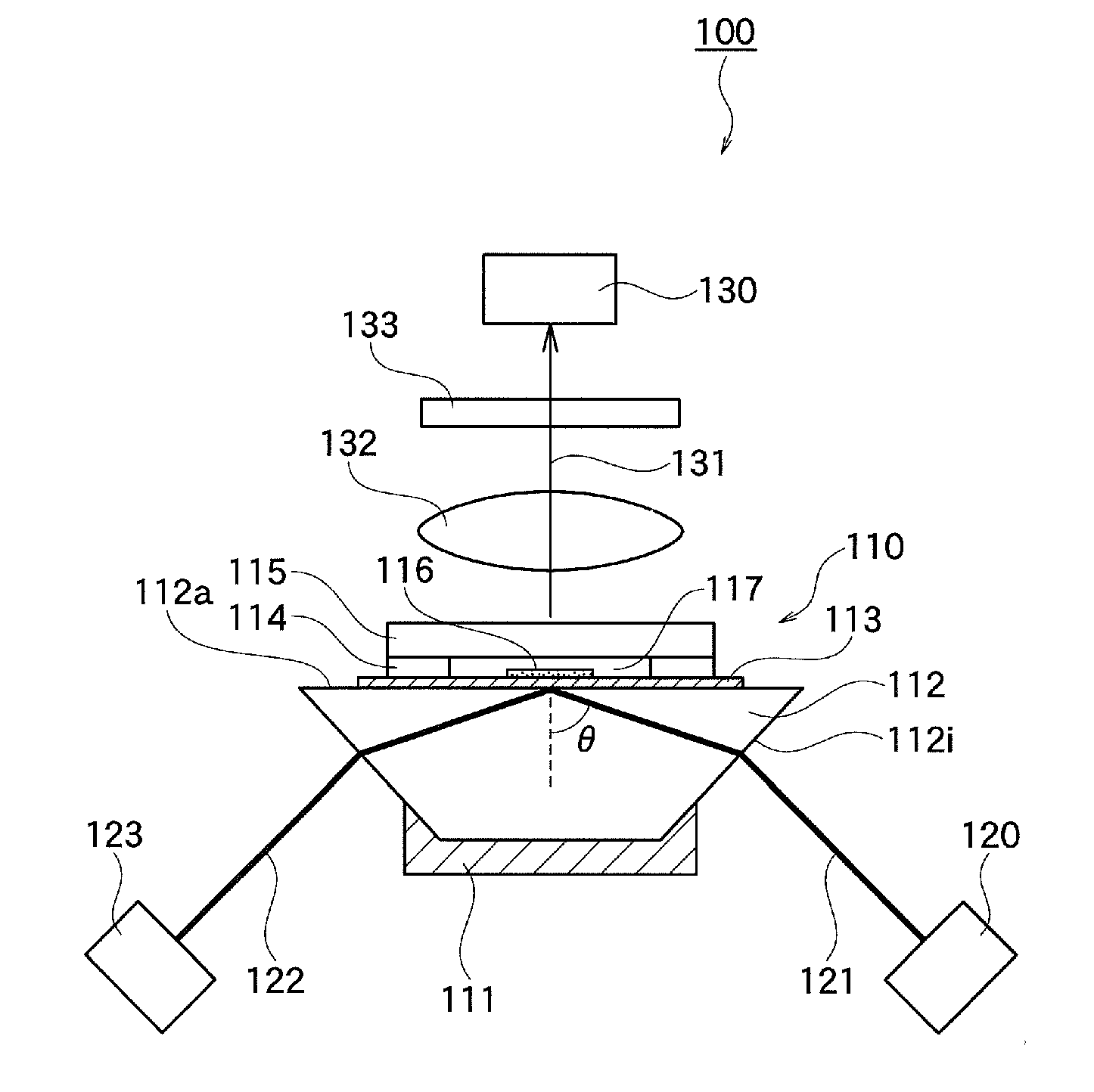
[0080]Step (a): First, on the main surface of a prism member having a substantially trapezoidal cross-section which was prepared using a cycloolefin polymer resin ZEONEX (registered trademark, manufactured by ZEON Corporation) as a material of a dielectric member, a chromium thin film was formed by sputtering, and a gold thin film was further formed on the surface of the chromium thin film by sputtering. The thickness of the chromium thin film was 1 to 3 nm and that of the gold thin film was 44 to 52 nm.

[0081]Step (b): The resulting prism on which these films were formed was immersed in an ethanol solution containing 1 mM of 10-carboxy-1-decanethiol for at least 24 hours to form a SAM (Self-Assembled Monolayer) on one side of the gold thin film. The prism was then removed from the solution and washed with ethanol and isopropanol, followed by drying using an air gun.

[0082]Step (c): On one end of a cylindrical member that was made of a polymethyl methacry...

example 2

(1) Preparation of Sensor Chip

[0100]Step (a): A prism having a gold film formed thereon was prepared in the same manner as in the step (a) of Example 1.

[0101]Step (b): A SAM (Self-Assembled Monolayer) was formed on one side of the gold thin film in the same manner as in Example 1.

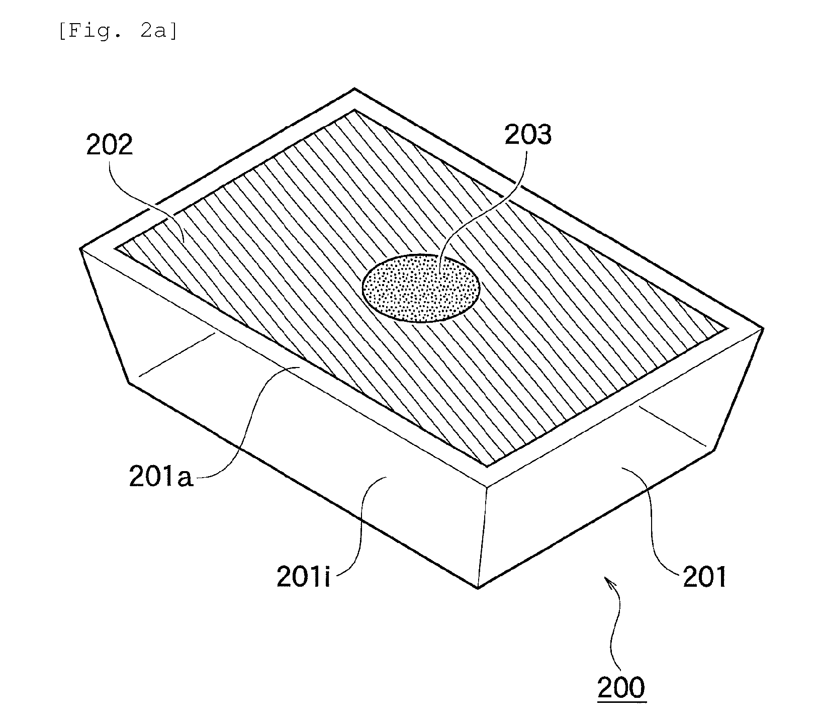
[0102]Step (c): The same solution-retaining member made of a polymethyl methacrylate resin (PMMA) as the one used in Example 1 was arranged at 3 spots (sensor sections of regions 1 to 3) on the above-prepared prism having a gold film and, in order to inhibit leakage from the solution-retaining member, the solution-retaining member and the prism were sandwiched by two stainless-steel plates from the top and bottom and then screw-fixed (on the upper stainless-steel plate, an opening through which reagents and the like were supplied to and removed from the solution-retaining member was arranged).

[0103]Step (d): Next, 0.2 mL of MES [2-morpholinoethanesulfonic acid]-buffered physiological saline (pH 6.0) contain...


PUM

PropertyMeasurementUnit
thicknessaaaaaaaaaa
thicknessaaaaaaaaaa
thicknessaaaaaaaaaa

Abstract

A sensor chip for surface plasmon-field enhanced spectroscopy, the sensor chip including: a dielectric member; a metal thin film formed on a main surface of the dielectric member; and a region on a part of the metal thin film, where a capturing substance that specifically captures a substance to be measured is immobilized. A blocking treatment with at least one blocking agent is performed in a region that includes the region where the capturing substance is immobilized, and the blocking treatment is not performed over an entirety of a wetted surface between a measurement sample and the metal thin film.

Description

TECHNICAL FIELD[0001]The present invention relates to a sensor chip for surface plasmon-field enhanced fluorescence spectroscopy, in which non-specific adsorption of contaminants originating from a measurement sample (biological sample) to a sensor section is inhibited. More particularly, the present invention relates to a sensor chip for surface plasmon-field enhanced fluorescence spectroscopy, in which non-specific adsorption of contaminants originating from a measurement sample (biological sample) to a sensor section is inhibited and generation of noise caused by autofluorescence generated from a dielectric member is reduced.BACKGROUND ART[0002]Detection and quantification of a tumor marker, a specific protein or nucleic acid or other biologically relevant substance contained in blood or urine of human or animal or in other biological sample are widely performed for diagnosis in today's medical field as well as for research in the fields of biology and biochemistry. As a method f...

Claims


Application Information

Patent Timeline
Patent Type & Authority Applications(United States)
IPC IPC(8): G01N21/64
CPCG01N21/648G01N33/54373
Inventor HIKAGE, NAOKIHIRAYAMA, HIROSHIWADA, TAKESHIAOKI, YOUICHI
Owner KONICA MINOLTA INC
Why Eureka
Try Eureka