Sidewall protection scheme for contact formation

a protection scheme and sidewall technology, applied in the direction of semiconductor/solid-state device details, electrical equipment, basic electric elements, etc., can solve the problems of high contact resistance, degradation of interfacial quality, and increase of recessed features cd, so as to prevent the loss of cd

Active Publication Date: 2016-12-29
TOKYO ELECTRON LTD
View PDF3 Cites 11 Cited by
  • Summary
  • Abstract
  • Description
  • Claims
  • Application Information

AI Technical Summary

Benefits of technology

[0005]Embodiments of the invention provide sidewall protection of recessed fea

Problems solved by technology

These residues can be nonvolatile, chemically and thermally stable, and if not removed, they can result in high contact resistance and degradation of interfacial quality.
Althoug

Method used


Image

  • Sidewall protection scheme for contact formation
  • Sidewall protection scheme for contact formation
  • Sidewall protection scheme for contact formation

Examples


Embodiment Construction

[0020]Embodiments of the invention provide a method for sidewall protection to prevent loss of CD during a cleaning process.

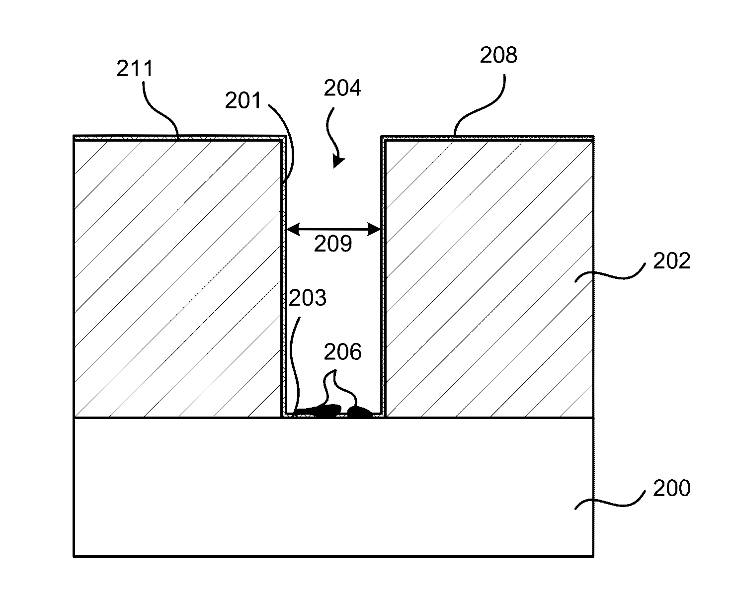
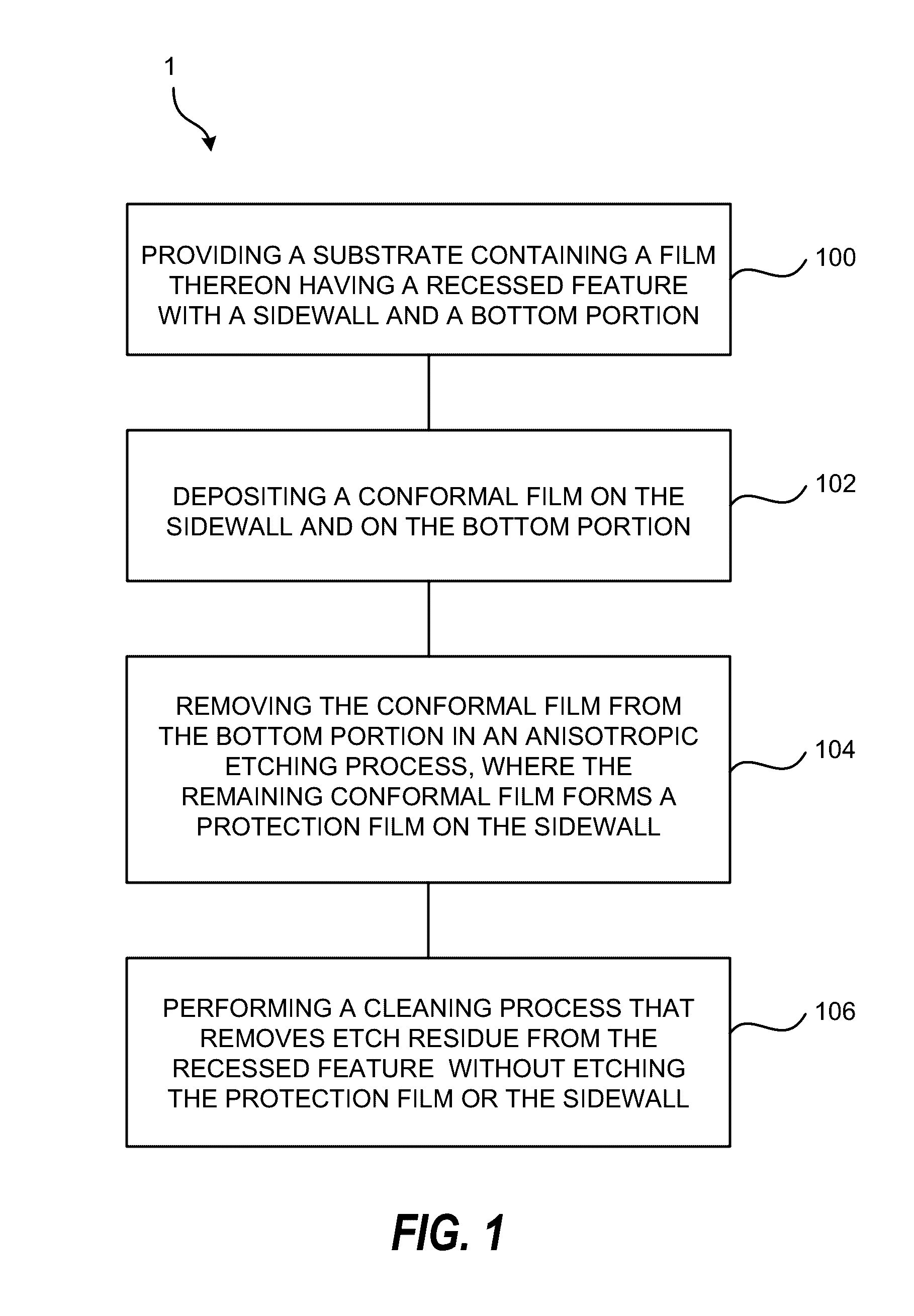
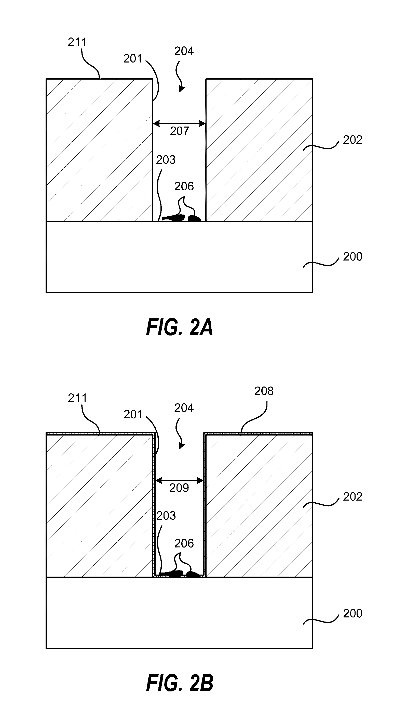
[0021]FIG. 1 is a process flow diagram for processing a substrate according to an embodiment of the invention, and FIGS. 2A-2E schematically show through cross-sectional views a method of processing a substrate according to an embodiment of the invention. The process flow 1 includes in 100, providing a substrate 200 containing a film 202 thereon having a recessed feature 204 with a sidewall 201 and a bottom portion 203. The recessed feature 204 can, for example, have a width 207 that is less than 200 nm, less than 100 nm, less than 50 nm, less than 25 nm, less than 20 nm, or less than 10 nm. In other examples, the recessed feature 204 can have a width 207 that is between 5 nm and 10 nm, between 10 nm and 20 nm, between 20 nm and 50 nm, between 50 nm and 100 nm, between 100 nm and 200 nm, between 10 nm and 50 nm, or between 10 nm and 100 nm. The width 207 can al...


PUM


Abstract

Method of manufacturing a semiconductor device is described that uses sidewall protection of a recessed feature to prevent loss of critical dimension during a cleaning process to remove etch residue. According to one embodiment, the method includes providing a substrate containing a film thereon having a recessed feature with a sidewall and a bottom portion, depositing a conformal film on the sidewall and on the bottom portion, removing the conformal film from the bottom portion in an anisotropic etching process, where the remaining conformal film forms a protection film on the sidewall, and performing a cleaning process that removes etch residue from the recessed feature without etching the protection film or the sidewall.

Description

CROSS-REFERENCE TO RELATED APPLICATIONS[0001]This application is related to and claims priority to U.S. Provisional Application No. 62 / 184,003, filed Jun. 24, 2015, the entire contents of which are herein incorporated by reference.FIELD OF INVENTION[0002]The present invention relates to the field of semiconductor manufacturing and semiconductor devices, and more particularly, to sidewall protection to prevent loss of critical dimension during a cleaning process.BACKGROUND OF THE INVENTION[0003]Current and future generations of metal-oxide-semiconductor field-effect transistors (MOSFETs) require tight control of parasitic capacitance while simultaneously optimizing metal-semiconductor contact resistance. In FinFET structures, maximizing the contact area can be achieved by creating a contact that wraps around the fin or by growing faceted epitaxial contacts, and then wrapping metal around the faceted epitaxial contact. For both MOSFET and FinFET processing, extensive etching and clean...

Claims


Application Information

Patent Timeline
IPC IPC(8): H01L21/768H01L21/02H01L21/311H01L21/306
CPCH01L21/76814H01L21/30604H01L21/02063H01L21/02271H01L21/02178H01L21/02181H01L21/02189H01L21/02186H01L21/31122H01L21/0228H01L21/3086H01L21/31144H01L21/76816H01L21/76831H01L23/485
Inventor CLARK, ROBERT D.TAPILY, KANDABARA N.
Owner TOKYO ELECTRON LTD
Why Eureka
Try Eureka