Electronic device with touch sensor and driving method therefor

a technology of electronic devices and touch sensors, applied in static indicating devices, acquiring/reconfiguring fingerprints/palmprints, instruments, etc., can solve the problems of increasing the cost of a screen size, and affecting the usability or performance of the electronic device. , to achieve the effect of reducing the current consumption of the electronic device and preventing the degradation of usability or performan

Active Publication Date: 2017-01-26
SAMSUNG ELECTRONICS CO LTD
View PDF4 Cites 56 Cited by
  • Summary
  • Abstract
  • Description
  • Claims
  • Application Information

AI Technical Summary

Benefits of technology

[0026]Accordingly, another aspect of the present disclosure is to operate a TSP and a fingerprint sensor together, based on mutual information between the TSP and the fingerprint sensor, and thus prevent a degradation of the usability or performance, due to mutual interference of the TSP and the fingerprint sensor.
[0027]Accordingly, another aspect of the present disclosure is to selectively drive the Tx and Rx of a fingerprint sensor to reduce current consumption in the electronic device According to an aspect of the present disclosure, an electronic device having a fingerprint verification function, is provided.

Problems solved by technology

The most prominent are a fingerprint recognition rate and a large current consumption.
First, a cost increase resulting from an increase to a screen size may occur. The fingerprint sensor should accurately scan a shape of the fingerprint of a finger differently from a capacitance type touch screen. For example, the fingerprint sensor may have Tx and Rx distances of 50 μm. Tx and Rx distance formations of a considerably dense interval-type are necessary in this process.
A screen of an electronic device such as a smart phone has a tendency to be large, and thus when a fingerprint sensor corresponding to the size of the screen is included in the electronic device, a cost is naturally increased according to the size o

Method used


Image

  • Electronic device with touch sensor and driving method therefor
  • Electronic device with touch sensor and driving method therefor
  • Electronic device with touch sensor and driving method therefor

Examples


Embodiment Construction

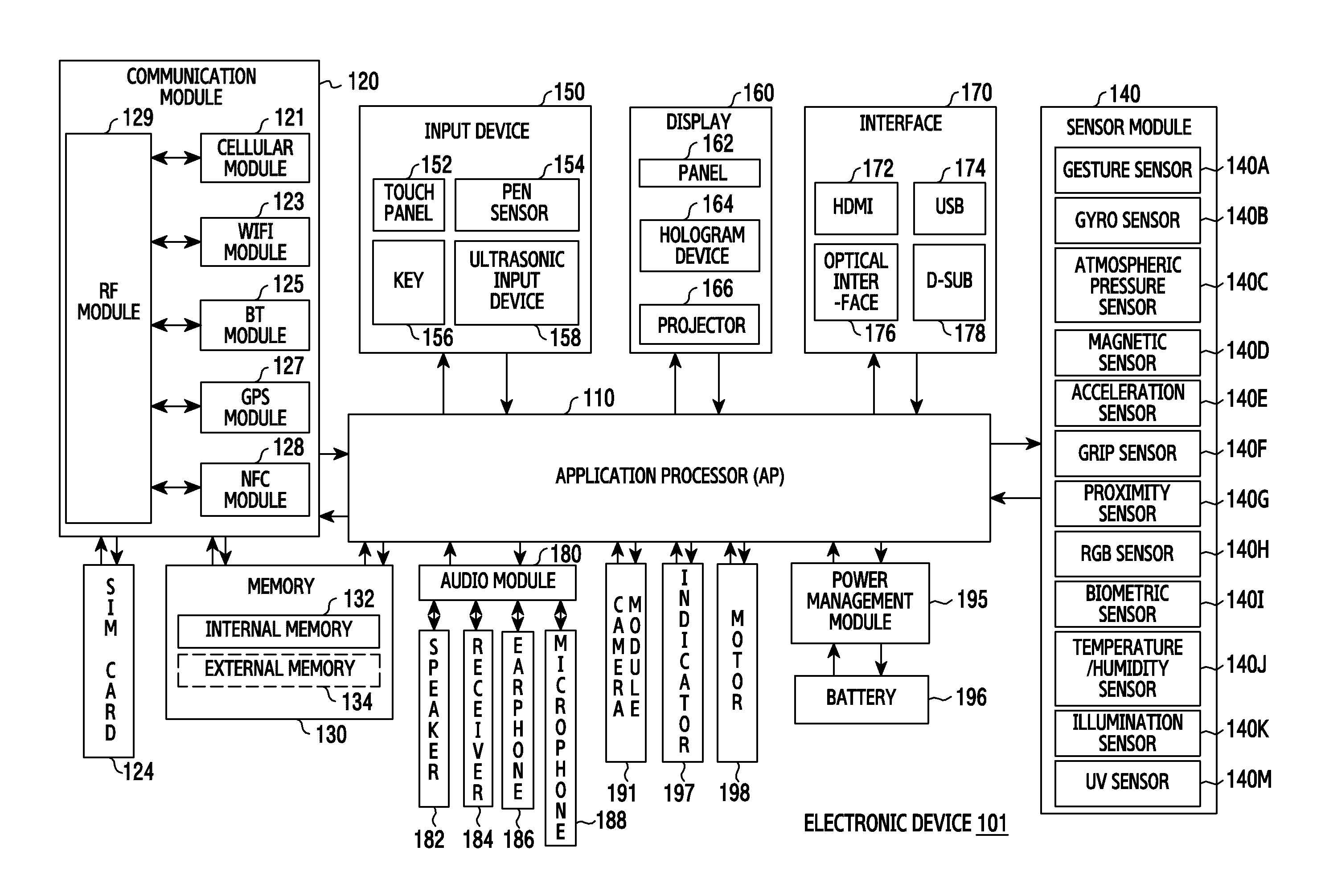
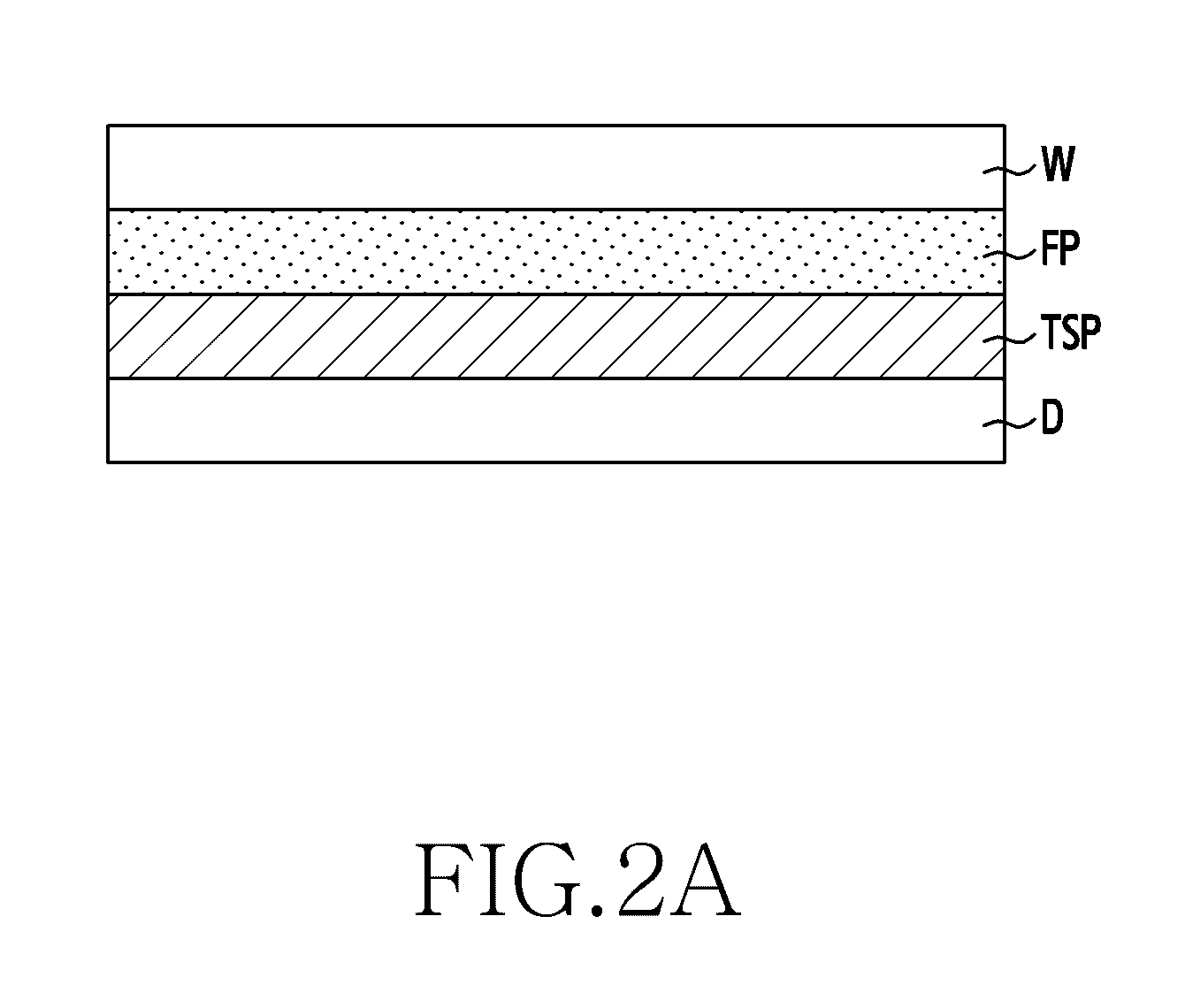
[0064]Hereinafter, various embodiments of the present disclosure will be explained with reference to the accompanying drawings. Although specific embodiments of the present disclosure are illustrated in the drawings and relevant detailed descriptions are provided, various changes can be made and various embodiments may be provided. Accordingly, various embodiments of the present disclosure are not limited to the specific embodiments and should be construed as including all changes and / or equivalents or substitutes included in the ideas and technological scopes of embodiments of the present disclosure. In the explanation of the drawings, similar reference numerals are used for similar elements.

[0065]The terms “include” and “may include”, as used herein, indicate the presence of disclosed corresponding functions, operations, elements, and the like, and do not limit additional functions, operations, elements, and the like. In addition, it should be understood that the terms “include” a...


PUM


Abstract

An electronic device having a fingerprint verification function is provided. The electronic device includes a display; a touch recognition sensor pattern for recognizing a touch input on the display; a fingerprint recognition sensor pattern for recognizing a fingerprint input on the display; and a processor functionally connected to the display, the touch recognition sensor pattern and the fingerprint recognition sensor pattern. The processor determines whether a fingerprint recognition mode is executed, and selectively activates the touch recognition sensor pattern and the fingerprint recognition sensor pattern according to whether the determined fingerprint recognition mode is executed.

Description

PRIORITY[0001]This application claims priority under 35 U.S.C. §119(a) to Korean Patent Application Serial No. 10-2015-0017963, which was filed in the Korean Intellectual Property Office on Feb. 5, 2015, the entire content of which is incorporated herein by reference.BACKGROUND[0002]1. Field of the Disclosure[0003]The present disclosure relates generally to an electronic device including a touch sensor including a fingerprint recognition (or fingerprint verification) in the electronic device and a method of driving the touch sensor.[0004]2. Description of the Related Art[0005]As use of electronic devices such as a smart phone, a tablet PC, and a wearable device is generalized, a concern about security and the usability of the electronic device increases. In fact, the security and the usability has a trade-off relationship, and thus it is normal that the usability is reduced while the security is increased. However, if a two-dimensional (2D) fingerprint sensor is installed together w...

Claims


Application Information

Patent Timeline
IPC IPC(8): G06K9/00G06F3/0488G09G3/36G06F3/041G09G3/3208G06V30/144
CPCG06K9/0002G06K9/00087G06F3/041G09G3/3208G06F2203/04112G06K9/0008G06F3/04883G06F2203/04106G09G2330/021G09G3/36G06F3/0412G06V40/13G06F21/32G06V40/1306G06F3/04166G06V40/1359G06V40/1365
Inventor CHO, JEONG-HOPARK, JEONG-MINBAE, DONG-HWANBAEK, SEUNG-GEOLSUH, JUNG-WONLEE, CHEOL-JUNCHUNG, DO-HYOUNGCHOI, KYONG-GON
Owner SAMSUNG ELECTRONICS CO LTD
Why Eureka
Try Eureka