Supercharge Your Innovation With Domain-Expert AI Agents!

Method for on/off control of switch, and switch circuit

a switch and switch circuit technology, applied in the direction of pulse duration/width modulation, instruments, electric digital data processing, etc., can solve the problems of processing load, timer interrupt processing may delay, and error may occur in the duty of pwm signal, so as to reduce processing load

Inactive Publication Date: 2017-02-16
AUTONETWORKS TECH LTD +2
View PDF4 Cites 2 Cited by
  • Summary
  • Abstract
  • Description
  • Claims
  • Application Information

AI Technical Summary

Benefits of technology

The patent is about a method for controlling the switching of a switch using third data. By updating the transfer source address where the third data is written, the switch can be controlled at different phases. This allows for easier and more efficient control of the switch without needing to search for a new transfer source address each time. The technical effect is to reduce the processing load and improve the efficiency of controlling the switch.

Problems solved by technology

Furthermore, when the CPU is in an interrupt-disabled state for example, timer interrupt processing may delay, and an error may occur in duty of the PWM signal.
However, according to the technique disclosed in the Infineon Reference, since the CPU needs to write the commands for one period for use in PWM control to the memory, and then to set and start DMA transfer, a processing load of generating the commands for one period and writing the generated commands to the memory is still not light.

Method used


Image

  • Method for on/off control of switch, and switch circuit
  • Method for on/off control of switch, and switch circuit
  • Method for on/off control of switch, and switch circuit

Examples


embodiment 1

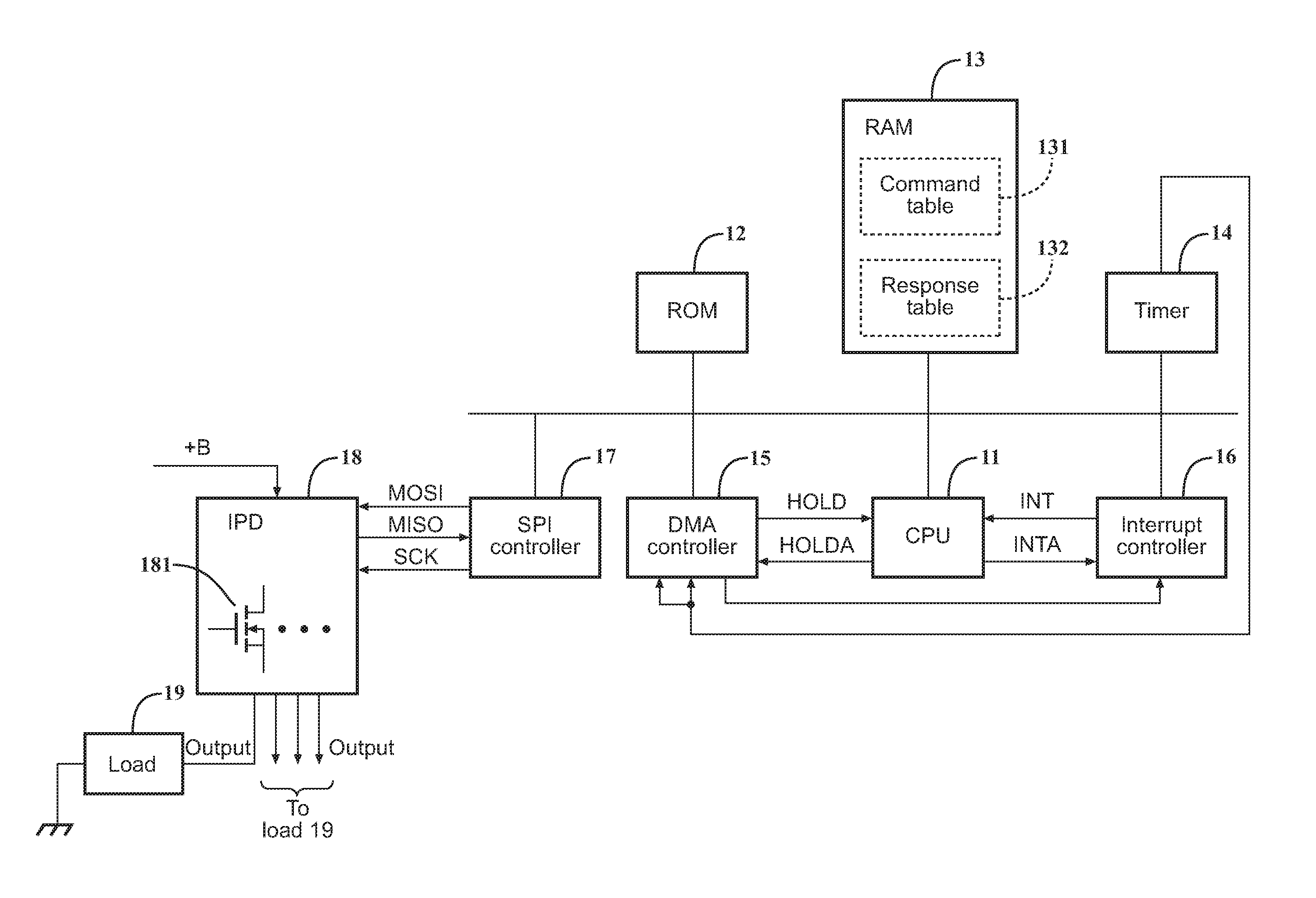
[0054]FIG. 1 is a block diagram illustrating an example of a configuration of a switch circuit according to Embodiment 1 of the present invention. The switch circuit includes a microcomputer having a CPU 11. The CPU 11 is connected, via a bus, to a ROM 12 for storing information such as a program, a RAM (that corresponds to a memory, a storage section, and a second storage section) 13 for temporarily storing information that has occurred, a timer 14 for generating a fixed-periodic signal, a DMA controller 15 for controlling DMA transfer in accordance with a DMA request, an interrupt controller 16 for processing an interrupt request, and an SPI controller 17 for performing communication conforming to the SPI.

[0055]The switch circuit is also provided with an IPD (that corresponds to a switch) 18 including four MOSFETs (hereinafter, referred to simply as “FETs”) 181, and the SPI controller 17 and the IPD 18 are connected to each other via a master output / slave input (MOSI: Master Out S...

embodiment 2

[0090]In contrast to Embodiment 1 that has an aspect in which updating of phases at which the IPD 18 is controlled to be turned on / off is out of consideration, Embodiment 2 has an aspect in which the processing of Embodiment 1 is executed and then the phases at which the IPD 18 is controlled to be turned on / off are updated.

[0091]Because a hardware configuration of a switch circuit according to Embodiment 2 is the same as that of Embodiment 1, like reference numerals are given to the corresponding components and redundant descriptions are omitted.

[0092]FIG. 5 is a diagram illustrating correspondence between commands and on / off control of the FET 181 of the switch circuit according to Embodiment 2 of the present invention. In FIG. 5, the horizontal axis denotes phases in a period in which the FET 181 is controlled to be turned on / off, and the figure shows, from the uppermost stage thereof, the content B, the content A, and content C of the command table 131 that are for controlling th...

embodiment 3

[0110]In contrast to Embodiment 1 that has an aspect in which an ON command and an OFF command are written only over the ON address and the OFF address in the command table 131 that respectively correspond to an ON phase and an OFF phase, Embodiment 3 has an aspect in which an ON command and an OFF command are written also over an address distanced from the ON address and the OFF address.

[0111]Because a hardware configuration of a switch circuit according to Embodiment 3 is the same as that of Embodiment 1, like reference numerals are given to the corresponding components and redundant descriptions are omitted.

[0112]FIGS. 7A and 7B are diagrams illustrating correspondence between commands and on / off control of a FET 181 of the switch circuit according to Embodiment 3 of the present invention. In FIGS. 7A and 7B, the horizontal axis denotes phases in a period in which the FET 181 is controlled to be turned on / off. FIGS. 7A and 7B respectively show, in the upper stage thereof, content...


PUM


Abstract

Realized are a switch on / off control method and a switch circuit that can reduce a processing load when controlling on / off of a switch whose various operations are controlled based on control data. All commands in a command table included in a RAM are DMA-transferred to an SPI controller, and the DMA-transferred commands are transmitted to an IPD via SPI communication, so as to perform on / off control. DIAG commands irrelevant to the on / off control of the IPD are written in advance in the entire region of the command table, transfer source addresses from which the commands are DMA-transferred to the IPD at phases at which the IPD is to be controlled to be turned on and off are calculated, and an ON command and an OFF command for controlling the IPD to be turned on and off are written over the diagnosis commands that were written in advance at the calculated transfer source addresses.

Description

CROSS-REFERENCE TO RELATED APPLICATIONS[0001]This application is the U.S. national stage of PCT / JP2015 / 056620 filed Mar. 6, 2015, which claims priority of Japanese Patent Application No. JP 2014-091944 filed Apr. 25, 2014.FIELD OF THE INVENTION[0002]The present invention relates to a switch on / off control method for being performed in a switch circuit that is provided with: a DMA controller for periodically DMA-transferring a plurality of pieces of transfer data in a memory; and a switch that is controlled to be turned on / off based on the transfer data from the DMA controller, and relates to the switch circuit.BACKGROUND[0003]In recent years, variety of switch circuits, called IPDs (Intelligent Power Devices), have been commercialized. IPDs have, for example, a function to protect a built-in switch from an overcurrent, a function to sense an electric current flowing through the switch, and the like. By controlling such an IPD to be turned on / off with a PWM signal to switch a power-s...

Claims


Application Information

Patent Timeline
Patent Type & Authority Applications(United States)
IPC IPC(8): G06F13/28G06F13/40
CPCG06F13/4022G06F13/28H03K7/08
Inventor KANAZAWA, AKIRAFURUTO, KENMESAKI, GENTAMAEDA, KAZUKI
Owner AUTONETWORKS TECH LTD
Features
  • R&D
  • Intellectual Property
  • Life Sciences
  • Materials
  • Tech Scout
  • Unparalleled Data Quality
  • Higher Quality Content
  • 60% Fewer Hallucinations
Learn More