Circuit board and display system

a display system and circuit board technology, applied in the field of circuit boards, can solve problems such as the difficulty of applying these mechanisms in the formation of mobile display devices, and achieve the effect of high-portability display systems

Active Publication Date: 2017-03-30
SEMICON ENERGY LAB CO LTD
View PDF5 Cites 20 Cited by
  • Summary
  • Abstract
  • Description
  • Claims
  • Application Information

AI Technical Summary

Benefits of technology

[0009]An object of one embodiment of the present invention is to provide a circuit board, a display device, an electronic device, or a display system in which the curvature of a display surface can be controlled. Another object of one embodiment of the present invention is to provide a lightweight circuit board, a lightweight display device, a lightweight electronic device, or a lightweight display system. Another object of one embodiment of the present invention is to provide a highly portable circuit board, a highly portable display device, a highly portable electronic device, or a highly portable display system. Another object of one embodiment of the present invention is to provide a novel circuit board, a novel display device, a novel electronic device, or a novel display system.
[0011]An embodiment of the present invention is a circuit board including a substrate and a curvature control mechanism. The curvature control mechanism includes a first electromagnet, a second electromagnet, an insulating film, and wirings. The substrate has flexibility. The first electromagnet and the second electromagnet are provided over a first surface of the substrate. The first electromagnet is provided so that a line connecting one magnetic pole and the other magnetic pole of the first electromagnet and a line parallel to a longitudinal direction of the substrate cross each other perpendicularly. The second electromagnet is provided so that a line connecting one magnetic pole and the other magnetic pole of the second electromagnet and the line parallel to the longitudinal direction of the substrate cross each other perpendicularly. The first electromagnet is provided so that a center axis of the first electromagnet is parallel to a center axis of the second electromagnet. The first electromagnet is provided so that a line connecting one magnetic pole of the first electromagnet and one magnetic pole of the second electromagnet and a line connecting the other magnetic pole of the first electromagnet and the other magnetic pole of the second electromagnet are parallel to the longitudinal direction of the substrate. The insulating film is provided over the substrate, the first electromagnet, and the second electromagnet. The wirings are electrically connected to the first electromagnet and the second electromagnet.
[0021]According to an embodiment of the present invention, a circuit board, a display device, an electronic device, or a display system in which the curvature of a display surface can be controlled can be provided. Alternatively, according to an embodiment of the present invention, a lightweight circuit board, a lightweight display device, a lightweight electronic device, or a lightweight display system can be provided. Alternatively, according to an embodiment of the present invention, a highly portable circuit board, a highly portable display device, a highly portable electronic device, or a highly portable display system can be provided. Alternatively, according to an embodiment of the present invention, a novel circuit board, a novel display device, a novel electronic device, or a novel display system can be provided.

Problems solved by technology

However, the display devices in Patent Document 1 and Patent Document 2 are stationary and the size, weight, or the like of the mechanism controlling the curvature of a display surface is not considered.
It is difficult to apply these mechanisms in forming mobile display devices in which the curvature of a display surface is controlled.

Method used


Image

  • Circuit board and display system
  • Circuit board and display system
  • Circuit board and display system

Examples


embodiment 1

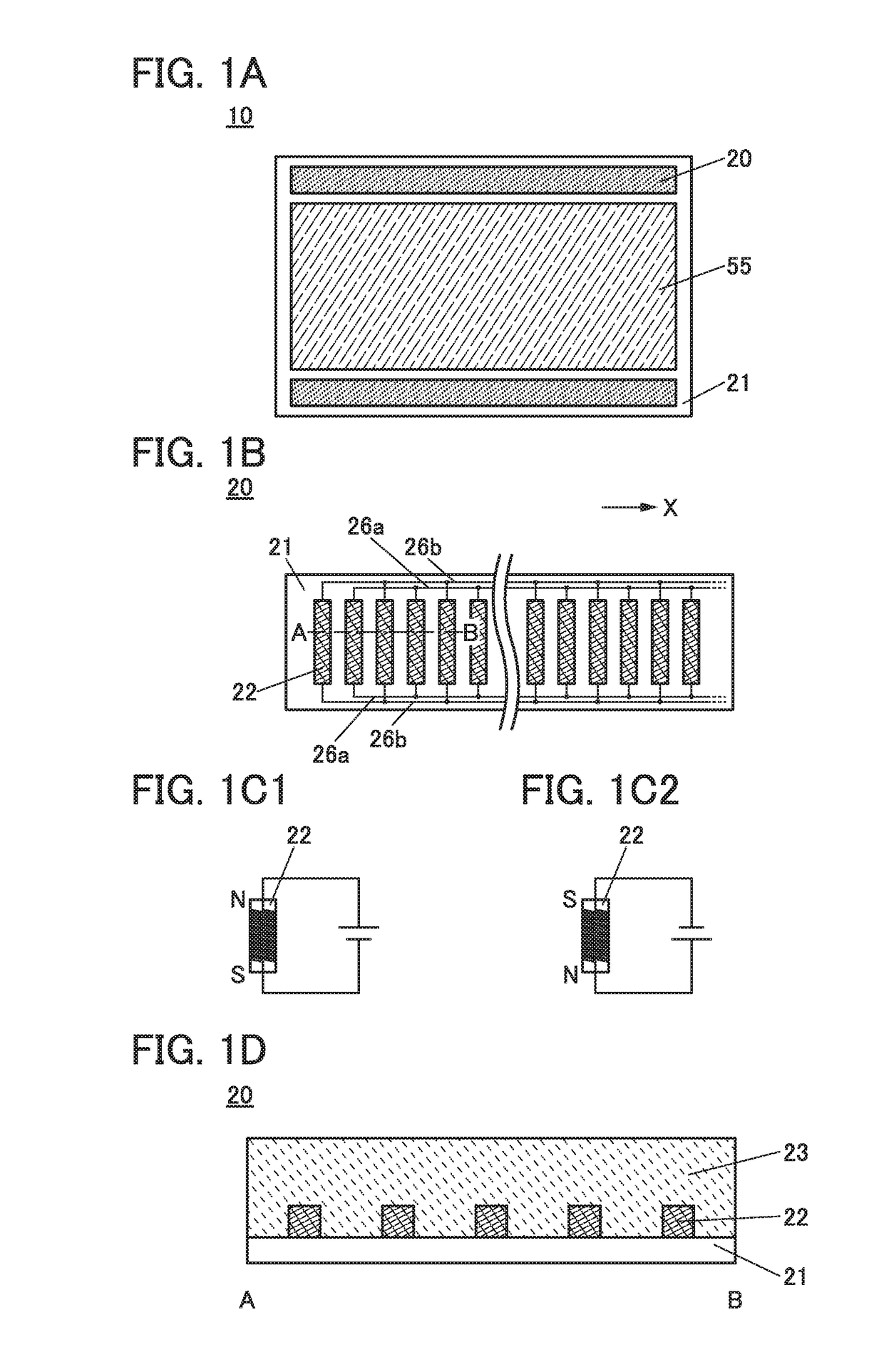
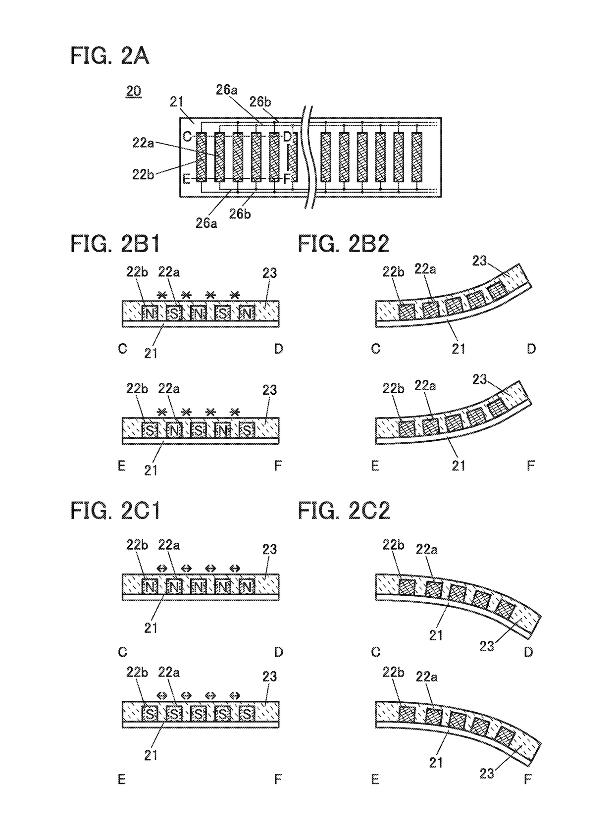
[0053]In this embodiment, a structure of a display device of one embodiment of the present invention is described with reference to FIGS. 1A, 1B, 1C1, 1C2, and 1D, FIGS. 2A, 2B1, 2B2, 2C1, and 2C2, FIGS. 3A to 3C, FIGS. 4A, 4B1, 4B2, and 4C, FIGS. 5A, 5B1, and 5B2, and FIGS. 6A1, 6A2, 6B1, and 6B2.

Structure Example 1 of Display Device

[0054]FIG. 1A is a top view of a display device 10. The display device 10 includes a substrate 21, a display portion 55, and curvature control mechanisms 20. The display portion 55 has a function of displaying an image. The display portion 55 includes a display element like a liquid crystal element, an EL (Electro Luminescence) element, or an electrophoretic element, for example.

[0055]The display portion 55 and the curvature control mechanisms 20 are provided over a first surface of the substrate 21. The curvature control mechanisms 20 are provided over a region of the display device 10 not overlapping with the display portion 55. The curvature control ...

embodiment 2

[0100]In this embodiment, a structure of a display device of one embodiment of the present invention is described with reference to FIGS. 7A to 7C, FIG. 8, FIGS. 9A, 9B1, and 9B2, and FIGS. 10A1 and 10A2. Note that the description of the display device 10 in Embodiment 1 can be referred to for structures which are similar to those of the display device 10 and which are included in a display device 70 in this structural example.

Structure Example of Display Device

[0101]FIG. 7A is a top view of the display device 70. The display device 70 includes the substrate 21, the display portion 55, and curvature control mechanisms 80. The display portion 55 has a function of displaying an image.

[0102]The display portion 55 is provided over the first surface of the substrate 21. The curvature control mechanisms 80 are provided in regions on the first surface side and the second surface side of the substrate 21 not overlapping with the display portion 55 of the display device 70. The curvature con...

embodiment 3

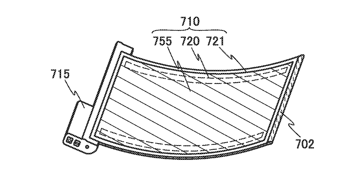
[0134]In this embodiment, an electronic device including the display device of one embodiment of the present invention will be described with reference to FIG. 11 and FIGS. 12A to 12E.

Structural Example of Electronic Device

[0135]FIG. 11 is a block diagram illustrating an example of the main structure of an electronic device 700. In FIG. 11, the directions of arrows represent the directions of signal transmission.

[0136]The electronic device 700 includes a display device 710 and a control circuit 750. The display device 710 includes a display portion 755 and a curvature control mechanism 720. The control circuit 750 includes a display control circuit 751 and a curvature control circuit 752.

[0137]The display portion 755 has a function of displaying an image, and the display control circuit 751 has a function of controlling image display of the display portion 755.

[0138]The curvature control mechanism 720 has a function of controlling the curvature of the display device 710. The curvatu...


PUM

PropertyMeasurementUnit
angleaaaaaaaaaa
angleaaaaaaaaaa
angleaaaaaaaaaa

Abstract

To provide a circuit board in which a curvature of a display surface can be controlled, or to provide a highly portable circuit board. A circuit board includes a substrate with flexibility and a curvature control mechanism. The curvature control mechanism includes a first electromagnet and a second electromagnet provided over a first surface of the substrate, an insulating film provided over the first and second electromagnets, and wirings electrically connected to the first and second electromagnets.

Description

BACKGROUND OF THE INVENTION[0001]1. Field of the Invention[0002]One embodiment of the present invention relates to a circuit board. Another embodiment of the present invention relates to a display device. Another embodiment of the present invention relates to an electronic device. Another embodiment of the present invention relates to a display system.[0003]Note that a circuit board in this specification means a general board that includes a circuit including wirings (e.g., a semiconductor device and a display device). In addition, a semiconductor device means a general device that can operate by utilizing semiconductor characteristics. Moreover, in this specification and the like, a display system means a general system including a display device. The display system may include a semiconductor device such as a transistor, an arithmetic device, a memory device, an imaging device, and the like, in addition to a display device.[0004]2. Description of the Related Art[0005]Display devic...

Claims


Application Information

Patent Timeline
Patent Type & Authority Applications(United States)
IPC IPC(8): G09G5/00H01F7/06H05K1/02G06F3/00G06F1/16
CPCG09G5/003G06F3/005G06F1/1686G06F1/1652H01F2007/062H01F7/064G09G2380/02G09G2354/00H05K1/028H01F2007/068G06F3/147H05K1/0268H05K1/05H05K1/165H05K2201/0116H05K2201/0133H05K2201/0162H05K2201/057H05K2201/086H05K2201/10128
Inventor SENDA, NAOYUKIYANAGISAWA, YUICHI
Owner SEMICON ENERGY LAB CO LTD
Why Eureka
Try Eureka