MEMS element including a stress decoupling structure and a component including such a MEMS element

a stress decoupling structure and element technology, applied in the direction of semiconductor devices, fluid speed measurement, instruments, etc., can solve the problems of severe impairment of the mems function, decoupling effect, and conventional stress decoupling structure, and achieve the effect of great vertical stress decoupling

Active Publication Date: 2017-04-06
ROBERT BOSCH GMBH
View PDF2 Cites 4 Cited by
  • Summary
  • Abstract
  • Description
  • Claims
  • Application Information

AI Technical Summary

Benefits of technology

[0018]It is a particular advantage if the mechanical connection between the MEMS layered structure and the carrier is designed to be offset outwards in relation to the trench structure in the MEMS substrate. In this case, neither the micromechanical function nor the stress decoupling of the MEMS element may be adversely affected by particles in the component surroundings. Moreover, in addition to the horizontal stress decoupling via the trench structure in the MEMS substrate, a vertical stress decoupling may be achieved via the layered structure. This vertical stress decoupling effect is particularly great if the functional element in the MEMS layered structure is mechanically decoupled from the MEMS layered structure in the connection area.

Problems solved by technology

In this process, stress effects occur, which may severely impair the MEMS function.
However, in practice, the conventional stress decoupling structure proves to be problematic in several respects.
Since the trench structure is applied in the rear side of the substrate, particles may collect in the trench structure during further processing, which may completely cancel the stress decoupling effect or at least significantly reduce it.
However, this is invariably associated with a significantly limited stress decoupling effect.
Depending on the thickness of the MEMS substrate, this is connected with comparatively high technical manufacturing complexity and is accordingly cost-intensive.
It has been shown that corners in the profile of the trench structure have an adverse effect on the stress decoupling effect.
In this case, neither the micromechanical function nor the stress decoupling of the MEMS element may be adversely affected by particles in the component surroundings.

Method used


Image

  • MEMS element including a stress decoupling structure and a component including such a MEMS element
  • MEMS element including a stress decoupling structure and a component including such a MEMS element
  • MEMS element including a stress decoupling structure and a component including such a MEMS element

Examples


Embodiment Construction

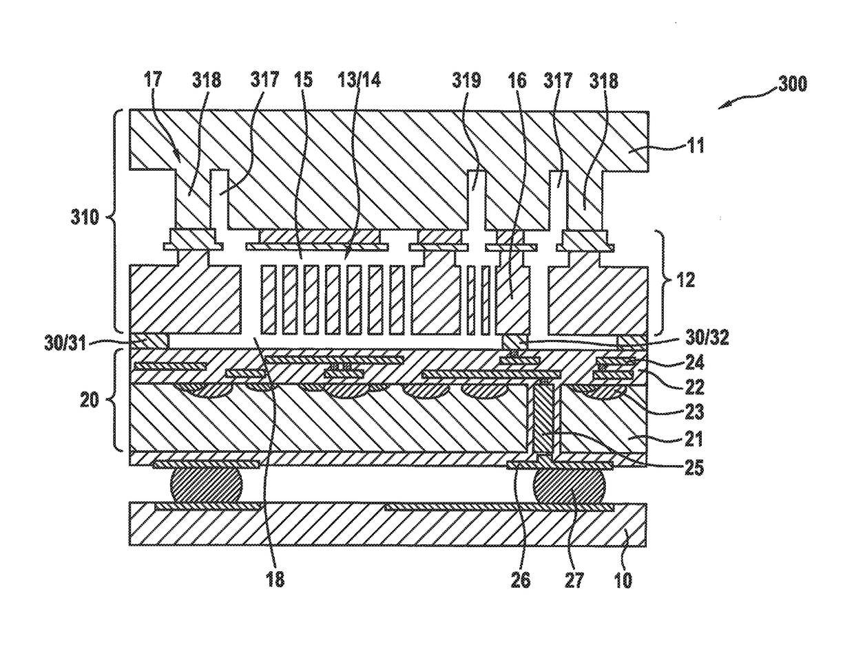
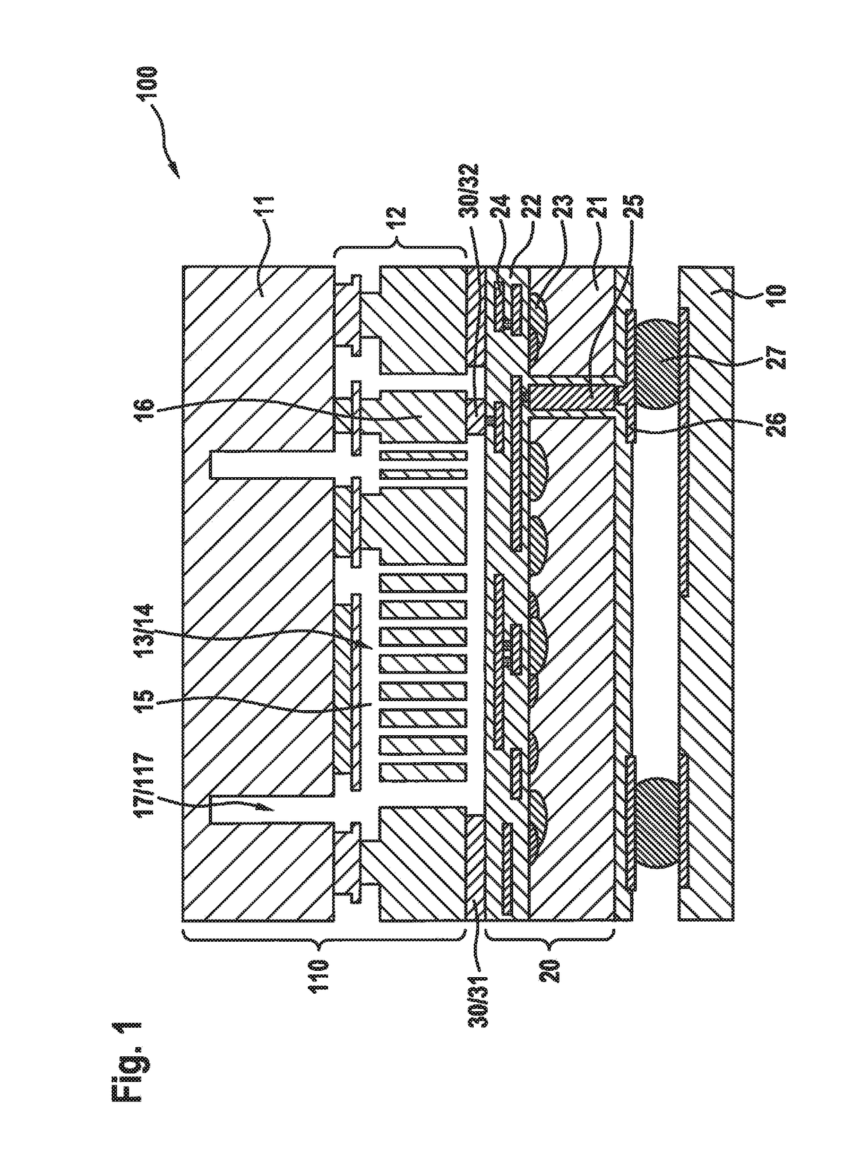
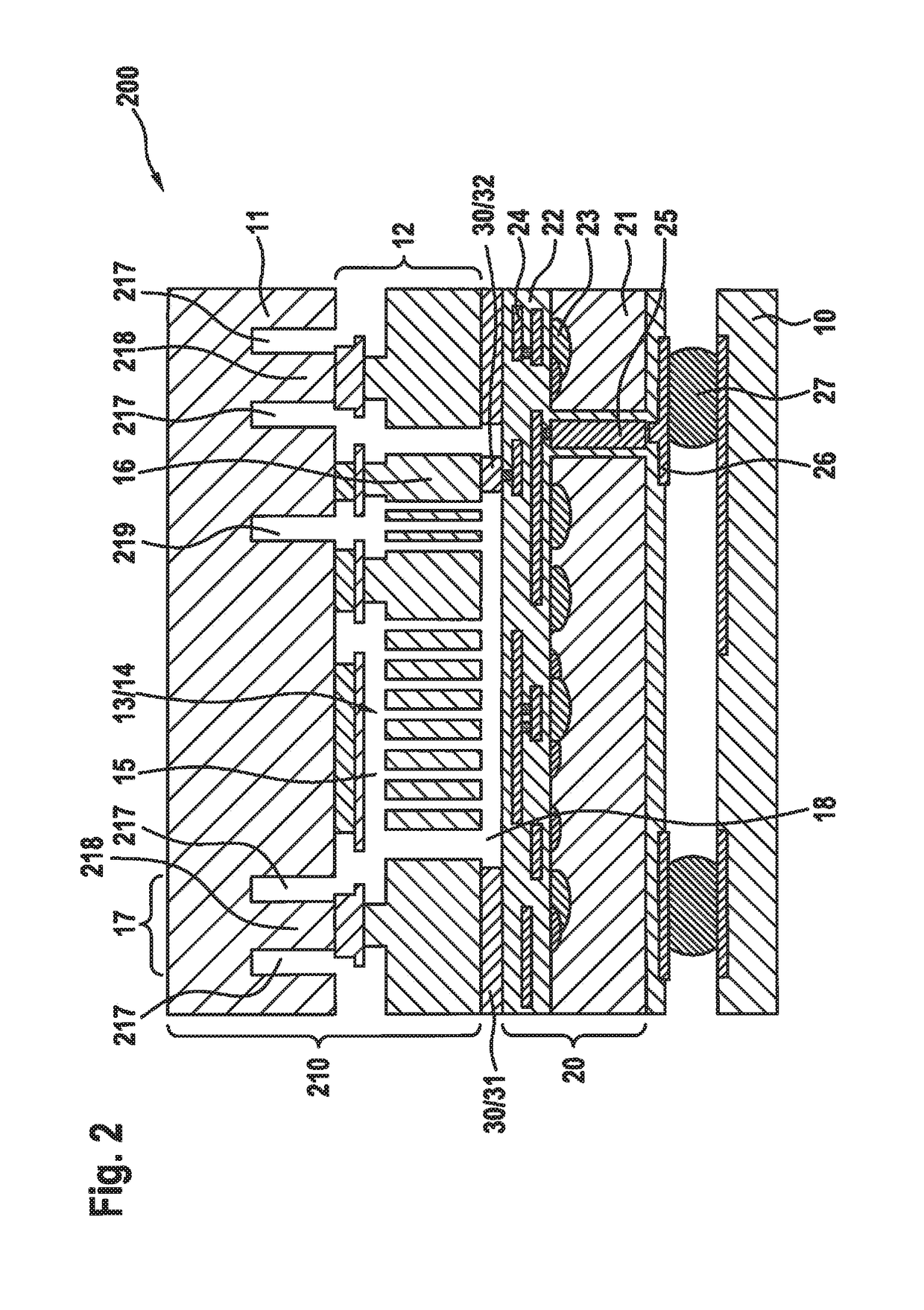
[0021]All three vertically hybrid integrated components 100, 200 and 300 shown in FIGS. 1 through 3 are mounted on an application circuit board 10 and include MEMS elements 110, 210 and 310 and an ASIC element 20. MEMS elements 110, 210 and 310 and ASIC element 20 are each assembled face-to-face, i.e., the active side of the MEMS chip, in which the sensor structure is formed, was connected to the active side of the ASIC chip, on which the circuit functions are implemented.

[0022]Sensor structures 13 of MEMS elements 110, 210 and 310 are identical. They include at least one deflectable functional element 14, which together with a signal detector, which are not indicated here in greater detail, are implemented in a layered structure 12 on a MEMS substrate 11. Another part of sensor structure 13 functions as an electrical terminal 16. In order to ensure the movability of this functional element 14, a space 15 is formed at least between functional element 14 and MEMS substrate 11. All ME...


PUM


Abstract

Measures are described which contribute simply and reliably to the mechanical decoupling of a MEMS functional element from the structure of a MEMS element. The MEMS element includes at least one deflectable functional element, which is implemented in a layered structure on a MEMS substrate, so that a space exists between the layered structure and the MEMS substrate, at least in the area of the functional element. According to the invention, a stress decoupling structure is formed in the MEMS substrate in the form of a blind hole-like trench structure, which is open to the space between the layered structure and the MEMS substrate and extends into the MEMS substrate to only a predefined depth, so that the rear side of the MEMS substrate is closed, at least in the area of the trench structure.

Description

BACKGROUND INFORMATION[0001]The present invention relates to a MEMS element including at least one deflectable functional element, which is implemented in a layered structure on a MEMS substrate, so that a space exists between the layered structure and the MEMS substrate, at least in the area of the functional element, and including a stress decoupling structure, which is formed in the MEMS substrate. Furthermore, the present invention relates to a component including such a MEMS element.[0002]MEMS elements may be used, for example, as sensor elements for detecting and measuring accelerations, rotation rates, magnetic fields and pressures for the most varied applications, for example, in the automotive technology and consumer segment. Particular emphasis is placed on miniaturization of the elements and components including high function integration. In this respect, so-called bare die or chip scale packages prove to be particularly advantageous, since repackaging of the chips is omi...

Claims


Application Information

Patent Timeline
Patent Type & Authority Applications(United States)
IPC IPC(8): B81B7/00
CPCB81B7/0048B81B2207/07B81B2207/012H01L2224/16225
Inventor CLASSEN, JOHANNESREINMUTH, JOCHENHATTASS, MIRKOREICHENBACH, RALFPUYGRANIER, ANTOINE
Owner ROBERT BOSCH GMBH
Why Eureka
Try Eureka