

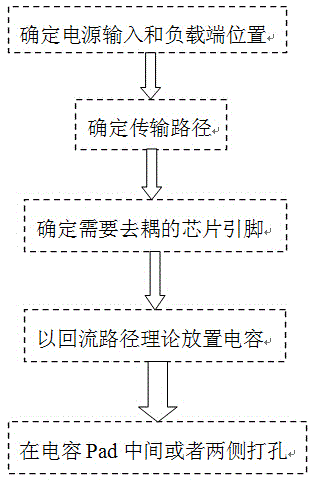
Via hole design method for improving capacitor decoupling effect
A design method and capacitor technology, applied in the field of electronics, can solve the problems of affecting the performance of PCB power supply, discount of capacitor decoupling effect, large capacitor return path, etc., to achieve the effect of improving design quality, reducing design space and simple operation
- Summary
- Abstract
- Description
- Claims
- Application Information
AI Technical Summary
Problems solved by technology
Method used
Image

Examples
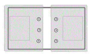
example 1
[0027] Example 1. The type of capacitor package is relatively large, and a via hole can be placed between the two capacitor pads;
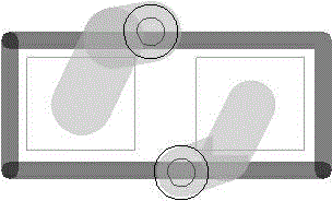
example 2
[0028] Example 2: The package type of the capacitor is small, and a via cannot be placed between the two capacitor pads.
[0029] By analyzing the position of the capacitor via hole, find out the placement method that is most conducive to reducing the loop area, so as to optimize the decoupling effect.
[0030] Such as figure 2 As shown, by punching the via hole of the large package capacitor on the inside of the capacitor pad.
[0031] Such as image 3 As shown, the vias of the capacitors in the small package are punched on both sides of the capacitor pad.
[0032] In this way, the parasitic inductance of the leads and the plane (power supply and ground) is greatly reduced, and at the same time, the return path of the capacitor is greatly reduced, the decoupling effect of the capacitor is greatly enhanced, and the wiring space of the capacitor is reduced, saving PCB layout space. It reduces the risk of PCB board components not being placed properly.
[0033] The impact...
PUM
 Abstract
Description
Claims
Application Information