Unlock instant, AI-driven research and patent intelligence for your innovation.

Array substrate, manufacturing method thereof and display device

a technology of array substrate and manufacturing method, applied in the field of array substrate, can solve the problems of reducing the contrast affecting the display effect of the display device, and leaking light of the display device, and achieve the effect of reducing the light leakage of the display devi

Active Publication Date: 2017-04-20
BOE TECH GRP CO LTD +1
View PDF2 Cites 3 Cited by
  • Summary
  • Abstract
  • Description
  • Claims
  • Application Information

AI Technical Summary

Benefits of technology

The technical effect of this patent is to provide a way to make a display that leaks less light than older displays, making it easier to see the pixels. This invention relates to a new way of making a display substrate, which can be used in devices like TVs and phones.

Problems solved by technology

However, the inventor of the present application found that, when the array substrate and the color filter substrate are quite misaligned along a direction in parallel with the extension direction of the gate line 3′, as shown in FIG. 2, the black matrix 5′ cannot fully shield the area between two adjacent pixel electrodes 1′, and as a result, light will be emitted out of the display device through the gaps 4′, which leads to light leakage of the display device, thereby reducing the contrast of the display device and influencing the display effect of the display device.

Method used


Image

  • Array substrate, manufacturing method thereof and display device
  • Array substrate, manufacturing method thereof and display device
  • Array substrate, manufacturing method thereof and display device

Examples


embodiment i

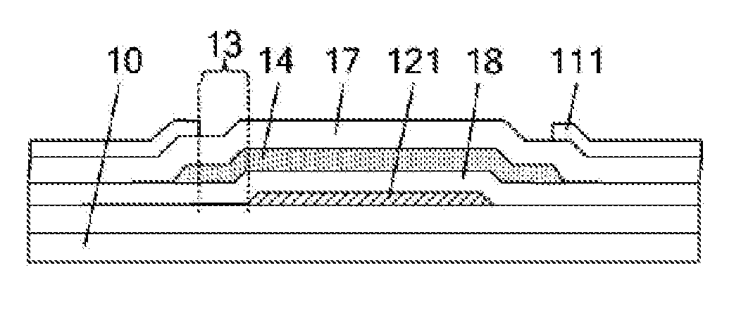
[0065]According to this embodiment of the present invention, an array substrate is provided. Specifically, as shown in FIGS. 3 and 4, the array substrate 1 comprises pixel regions 11 arranged in arrays, two adjacent ones of the pixel regions 11 having a signal line 12 arranged therebetween, and the pixel regions 11 and the signal line 12 having a gap 13 therebetween; wherein the array substrate 1 further comprises at least one light-leakage-proof electrode 14 arranged to be insulated from the pixel regions 11 and the signal line 12, and the vertical projection of the light-leakage-proof electrode 14 on the base substrate 10 at least covers a portion of the vertical projection of the gap 13 on the base substrate 10.

[0066]Exemplarily, the material of the light-leakage-proof electrode 14 can be a transparent conductive material such as indium tin oxide (ITO) or indium zinc oxide (IZO), or an opaque conductive material such as gold (Au), silver (Ag) or molybdenum (Mo). When the light-le...

embodiment ii

[0082]The present invention provides a manufacturing method for manufacturing the array substrate as mentioned in embodiment I. Specifically, the manufacturing method comprises the following steps.

[0083]Step S701: forming a signal line.

[0084]The step of forming a signal line may differ based on what kind of specific structure the signal line is. Exemplarily, when the signal line is a gate line, the step of forming a signal line comprises: forming a gate metal layer and forming a pattern comprising a gate line by a patterning process. When the signal line is a data line, the step of forming a signal line comprises: forming a source-drain metal layer and forming a pattern comprising a data line by a patterning process. When the signal line comprises both a gate line and a data line, the step of forming a signal line comprises: forming a gate metal layer and forming a pattern comprising a gate line by a patterning process, as well as forming a source-drain metal layer and forming a pat...


PUM

PropertyMeasurementUnit
conductiveaaaaaaaaaa
transparentaaaaaaaaaa
transparent conductiveaaaaaaaaaa

Abstract

The present invention relates to the field of display technology, and discloses an array substrate, a manufacturing method thereof and a display device, for reducing the light leakage of a display device. The array substrate comprises a plurality of pixel regions arranged in arrays on a base substrate, two adjacent ones of the pixel regions having a signal line arranged therebetween, and the pixel regions and the signal line having a gap therebetween, wherein the array substrate further comprises at least one light-leakage-proof electrode arranged to be insulated from the pixel regions and the signal line, and the vertical projection of the light-leakage-proof electrode on the base substrate at least covers a portion of the vertical projection of the gap on the base substrate. The present invention is applicable in the field of display technology.

Description

RELATED APPLICATIONS[0001]The present application claims the benefit of Chinese Patent Application No. 201510148163.9, filed on Mar. 31, 2015, the entire disclosure of which is incorporated herein by reference.FIELD OF THE INVENTION[0002]The present invention relates to the field of display technology, and in particular to an array substrate and a manufacturing method thereof, as well as a display device.BACKGROUND ART[0003]Currently, a common liquid crystal display device is a twisted nematic type liquid crystal display device in a normally white mode, the display device comprising an array substrate and a color filter substrate aligned with each other.[0004]Exemplarily, as shown in FIG. 1, the array substrate comprises a plurality of pixel electrodes 1 arranged in arrays, a data line 2′ situated between two adjacent columns of pixel electrodes 1′, and a gate line 3′ situated between two adjacent rows of pixel electrodes 1′, wherein the pixel electrodes 1′ and the data line 2′ have...

Claims


Application Information

Patent Timeline
Patent Type & Authority Applications(United States)
IPC IPC(8): G02F1/1343G02F1/1368G02F1/1362G02F1/1333
CPCG02F1/13439G02F1/133345G02F1/1368G02F1/136286G02F2203/66G02F2201/123G02F2001/136218G02F2201/121G02F2001/136295G02F1/134309H01L27/124H01L27/1259G02F1/136218G02F1/136209G02F1/1396G02F1/136295
Inventor DONG, ZHIFUXUE, WEISONG, PINGLI, HONGMIN
Owner BOE TECH GRP CO LTD