Nonvolatile memory devices and solid state drives including the same

a technology of nonvolatile memory and solid state drives, applied in the field of semiconductor memory devices, can solve the problem that content stored therein may be lost in the absence of power

Active Publication Date: 2017-04-20
SAMSUNG ELECTRONICS CO LTD
View PDF5 Cites 8 Cited by
  • Summary
  • Abstract
  • Description
  • Claims
  • Application Information

AI Technical Summary

Benefits of technology

[0007]According to an exemplary embodiment of the present inventive concept, a nonvolatile memory device includes a memory cell array, a voltage generator, and a control circuit. The voltage generator generates word-line voltages to be applied to the memory cell array. The control circuit generates control signals that control the voltage generator in response to a comman

Problems solved by technology

Volatile semiconductor memory devices may perform read and write operations at

Method used


Image

  • Nonvolatile memory devices and solid state drives including the same
  • Nonvolatile memory devices and solid state drives including the same
  • Nonvolatile memory devices and solid state drives including the same

Examples


Embodiment Construction

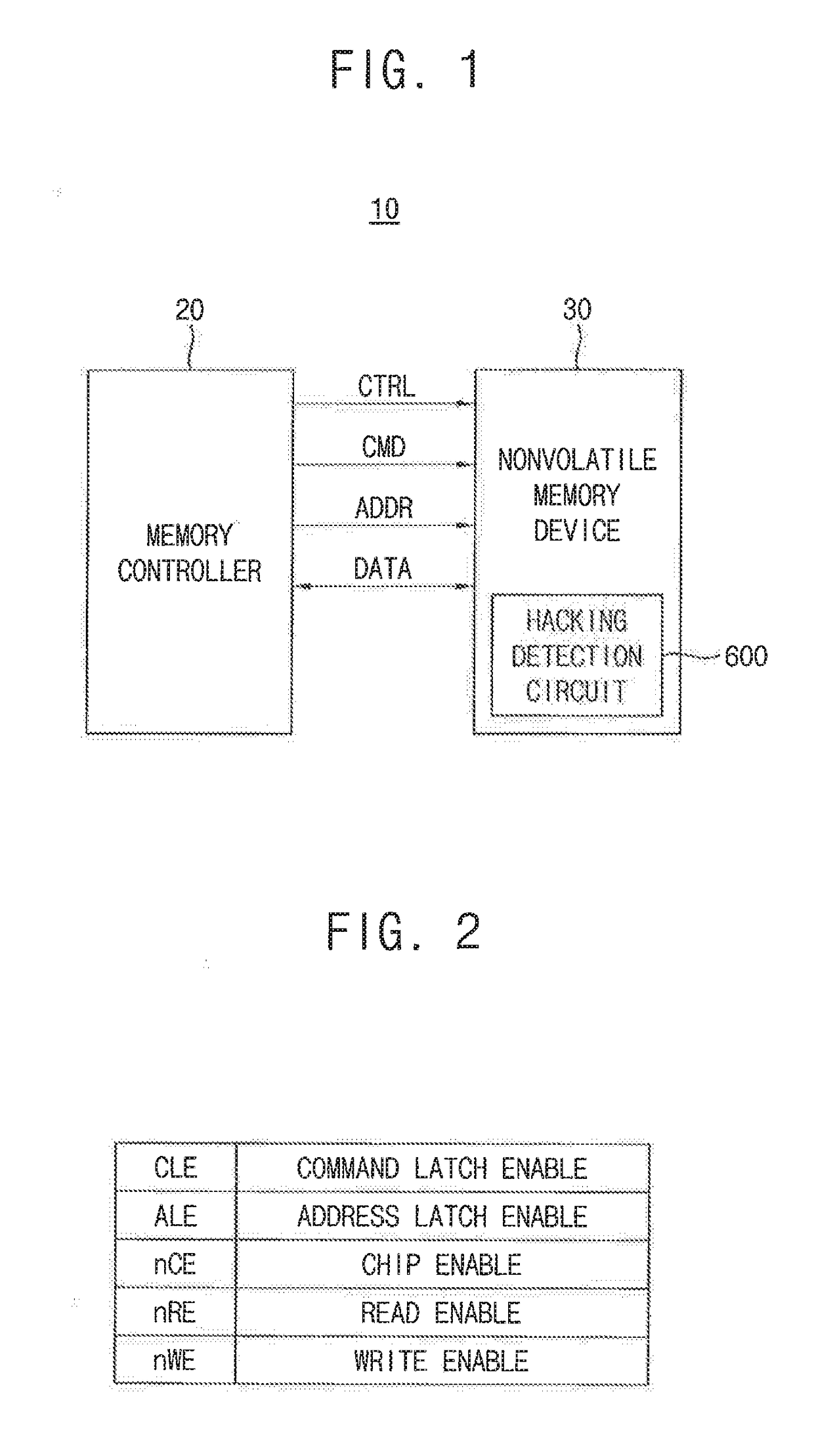
[0050]Exemplary embodiments of the present inventive concept will be described more fully hereinafter with reference to the accompanying drawings. The present inventive concept may, however, be embodied in many different forms and should not be construed as limited to the exemplary embodiments set forth herein. In the drawings, the sizes and relative sizes of layers and regions may be exaggerated for clarity. Like numerals may refer to like elements throughout this application. All elements shown in the drawings or hereinafter described may be composed of circuits.

[0051]It will be understood that when an element is referred to as being “connected” or “coupled” to another element, it can be directly connected or coupled to the other element or intervening elements may be present.

[0052]As used herein, the singular forms “a,”“an” and “the” are intended to include the plural forms as well, unless the context clearly indicates otherwise.

[0053]FIG. 1 is a block diagram illustrating a memo...


PUM


Abstract

A nonvolatile memory device includes a memory cell array, a voltage generator, and a control circuit. The voltage generator generates word-line voltages to be applied to the memory cell array. The control circuit generates control signals that control the voltage generator in response to a command and an address. The control circuit includes a hacking detection circuit. The hacking detection circuit disables an operation of the nonvolatile memory device when a hacking is detected, wherein the hacking is detected when an access sequence of the command and the address does not match a standard sequence of the nonvolatile memory device a consecutive number of times.

Description

CROSS-REFERENCE TO RELATED APPLICATION[0001]This U.S. non-provisional patent application claims priority under 35 U.S.C. §119 to Korean Patent Application No. 10-2015-0145049, filed on Oct. 19, 2015, in the Korean Intellectual Property Office (KIPO), the disclosure of which is incorporated by reference herein in its entirety.TECHNICAL FIELD[0002]Exemplary embodiments of the present inventive concept relate generally to semiconductor memory devices, and more particularly, to nonvolatile memory devices and solid state drives including the same.DISCUSSION OF THE RELATED ART[0003]Semiconductor memory devices may be classified as volatile semiconductor memory devices or nonvolatile semiconductor memory devices. Volatile semiconductor memory devices may perform read and write operations at high speed, while contents stored therein may be lost in the absence of power. Nonvolatile semiconductor memory devices may retain contents stored therein in the absence of power. For this reason, nonvo...

Claims


Application Information

Patent Timeline
IPC IPC(8): G06F21/55G11C16/22
CPCG11C16/22G06F21/556G11C16/0483G11C16/08G11C17/14G06F21/755Y04S40/20
Inventor KIM, JUNG-SOOJUNG, BONG-KIL
Owner SAMSUNG ELECTRONICS CO LTD
Why Eureka
Try Eureka