Semiconductor device including electromagnetic absorption and shielding

Active Publication Date: 2017-04-20
SANDISK INFORMATION TECH SHANGHAI
View PDF4 Cites 7 Cited by
  • Summary
  • Abstract
  • Description
  • Claims
  • Application Information

AI Technical Summary

Benefits of technology

[0067]In another embodiment, the present technology relates to a semiconductor device, comprising: a substrate; a solder mask layer on the substrate, the solder mask layer including a first absorbing material for absorbing at least one of EMI and RFI; one or more semiconductor die affixed and electrically connected to the substrate; a molding compound encapsulating at least the one or more semiconductor die; and a layer provided on the molding compound, the layer including a second absorbing material for absorbing at least one of EMI and RFI.
[0068]In a further embodiment, the present technology relates to a semiconductor device, comprising: a substrate; a solder mask layer on the substrate, the solder mask layer including a first absorbing material for absorbing at least one of EMI and RFI; one or more semiconductor die affixed and electrically conne

Problems solved by technology

In addition to the height of the bond wires 30 themselves, additional space must be left above the bond wires, as contact of the bond wires 30 of one die with the next die above may result in an electrical short.
EMI is the induction of electromagnetic radiation, which is emitted by electrical circuits carrying rapidly changing signals, as a by-product of their normal operation to other circuits, which causes unwanted signals (in

Method used


Image

  • Semiconductor device including electromagnetic absorption and shielding
  • Semiconductor device including electromagnetic absorption and shielding
  • Semiconductor device including electromagnetic absorption and shielding

Examples


Example

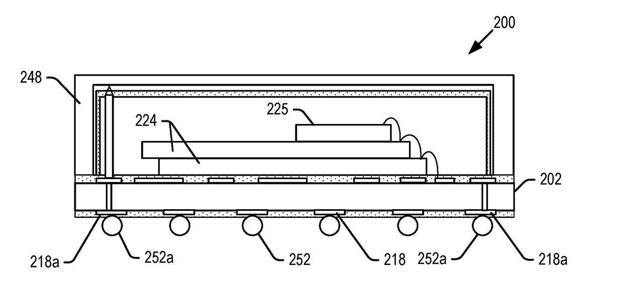
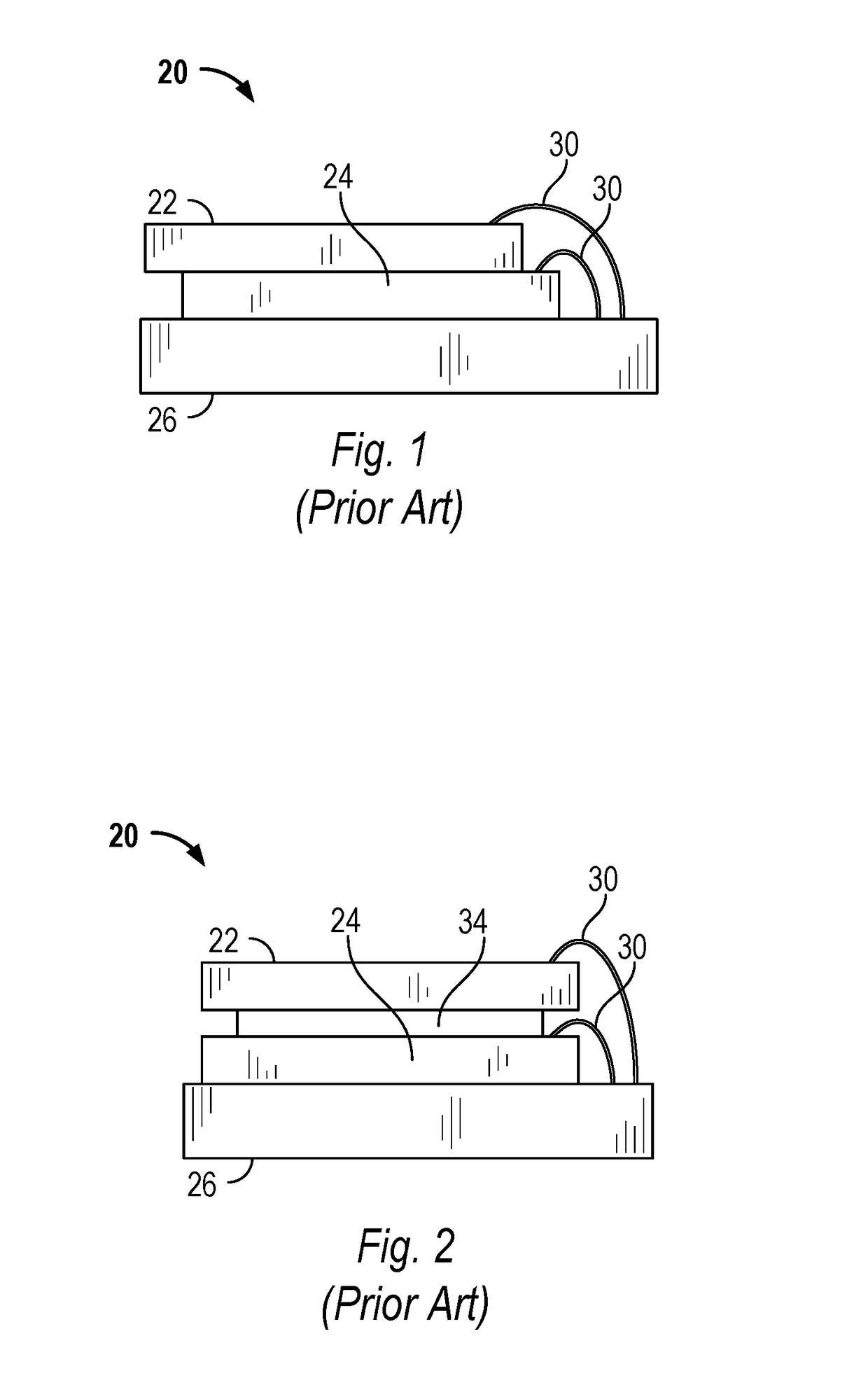
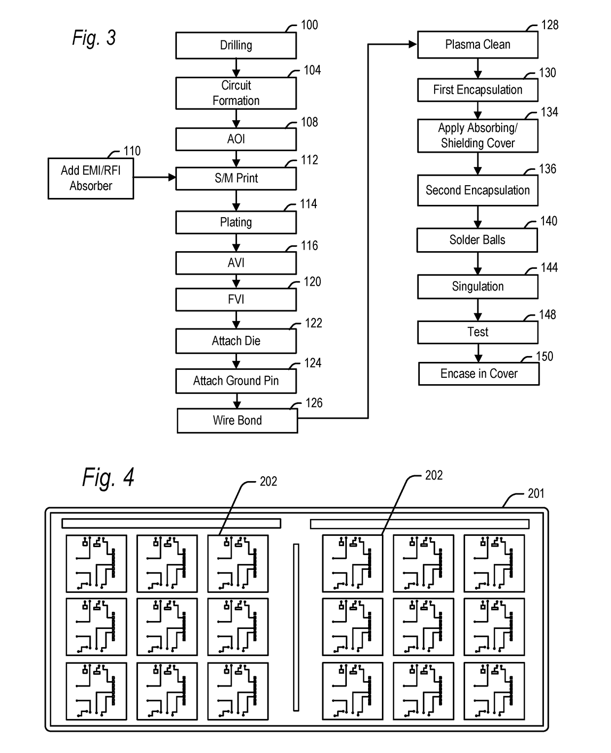
[0025]Embodiments will now be described with reference to FIGS. 3 through 18, which relate to a semiconductor package including EMI and RFI shielding and absorption. It is understood that the present invention may be embodied in many different forms and should not be construed as being limited to the embodiments set forth herein. Rather, these embodiments are provided so that this disclosure will be thorough and complete and will fully convey the invention to those skilled in the art. Indeed, the invention is intended to cover alternatives, modifications and equivalents of these embodiments, which are included within the scope and spirit of the invention as defined by the appended claims. Furthermore, in the following detailed description of the present invention, numerous specific details are set forth in order to provide a thorough understanding of the present invention. However, it will be clear to those of ordinary skill in the art that the present invention may be practiced wit...


PUM


Abstract

A semiconductor device is disclosed including material for absorbing EMI and/or RFI. The device includes a substrate, one or more semiconductor die, and molding compound around the one or more semiconductor die. The material for absorbing EMI and/or RFI may be provided within or on a solder mask layer on the substrate, or within a dielectric core of the substrate. The device may further include EMI/RFI-absorbing material around the molding compound and in contact with the EMI/RFI-absorbing material on the substrate to completely enclose the one or more semiconductor die in EMI/RFI-absorbing material.

Description

CLAIM OF PRIORITY[0001]This application is a divisional application of U.S. patent application Ser. No. 14 / 348,828, filed Mar. 31, 2014, which application is a 371 of International Patent Application No. PCT / CN2012 / 074737, filed Apr. 26, 2012, which applications are incorporated by reference herein in their entirety.BACKGROUND OF THE INVENTIONField of the Invention[0002]Embodiments of the present invention relate to semiconductor devices.Description of the Related Art[0003]The strong growth in demand for portable consumer electronics is driving the need for high-capacity storage devices. Non-volatile semiconductor memory devices, such as flash memory storage cards, are becoming widely used to meet the ever-growing demands on digital information storage and exchange. Their portability, versatility and rugged design, along with their high reliability and large capacity, have made such memory devices ideal for use in a wide variety of electronic devices, including for example digital c...

Claims


Application Information

Patent Timeline
IPC IPC(8): H01L23/31H01L25/00H01L23/552H01L25/065H01L21/56H01L23/498
CPCH01L23/3135H01L21/565H01L23/49811H01L23/552H01L2225/06562H01L25/50H01L2225/06506H01L2225/0651H01L2225/06537H01L25/0657H01L23/3121H01L23/49822H01L23/49827H01L25/18H01L2224/48091H01L2224/48145H01L2224/48147H01L2224/48227H01L2924/15311H01L2924/00014
Inventor HUANG, DACHENGBAI, YEQIAN, KAIYOUCHIU, CHIN-TIEN
Owner SANDISK INFORMATION TECH SHANGHAI
Why Eureka
Try Eureka