
Layout method for compound semiconductor integrated circuits

a technology of integrated circuits and semiconductors, applied in semiconductor devices, semiconductor devices, electrical devices, etc., can solve the problems of reducing affecting etc., to enhance the moisture resistance ability reduce the cost of the compound semiconductor integrated circuit, and efficiently remove the isolation layer

Active Publication Date: 2017-04-20
WIN SEMICON
View PDF4 Cites 0 Cited by
  • Summary
  • Abstract
  • Description
  • Claims
  • Application Information

AI Technical Summary

Benefits of technology

The present invention aims to solve two technical problems: the first one is that the removal of the wide range of an isolation layer of polyimide in a compound semiconductor integrated circuit can significantly enhance its moisture resistance ability. The second problem is that reducing the impact of the isolation layer on the impedance of the integrated circuit can also enhance its performance.

Problems solved by technology

However, since the polyimide itself has such a rate of water absorption that the existence of the polyimide isolation layer will seriously affect the moisture resistance ability of the compound semiconductor integrated circuit.
But the existence of the polyimide isolation layer in other wide area where does not need the polyimide isolation layer is the main reason that reduces the moisture resistance ability of the compound semiconductor integrated circuit.

Method used


Image

  • Layout method for compound semiconductor integrated circuits
  • Layout method for compound semiconductor integrated circuits
  • Layout method for compound semiconductor integrated circuits

Examples


Embodiment Construction

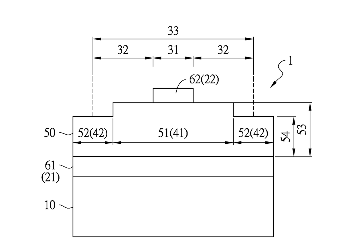
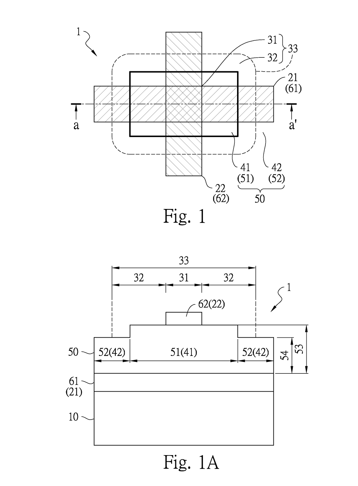
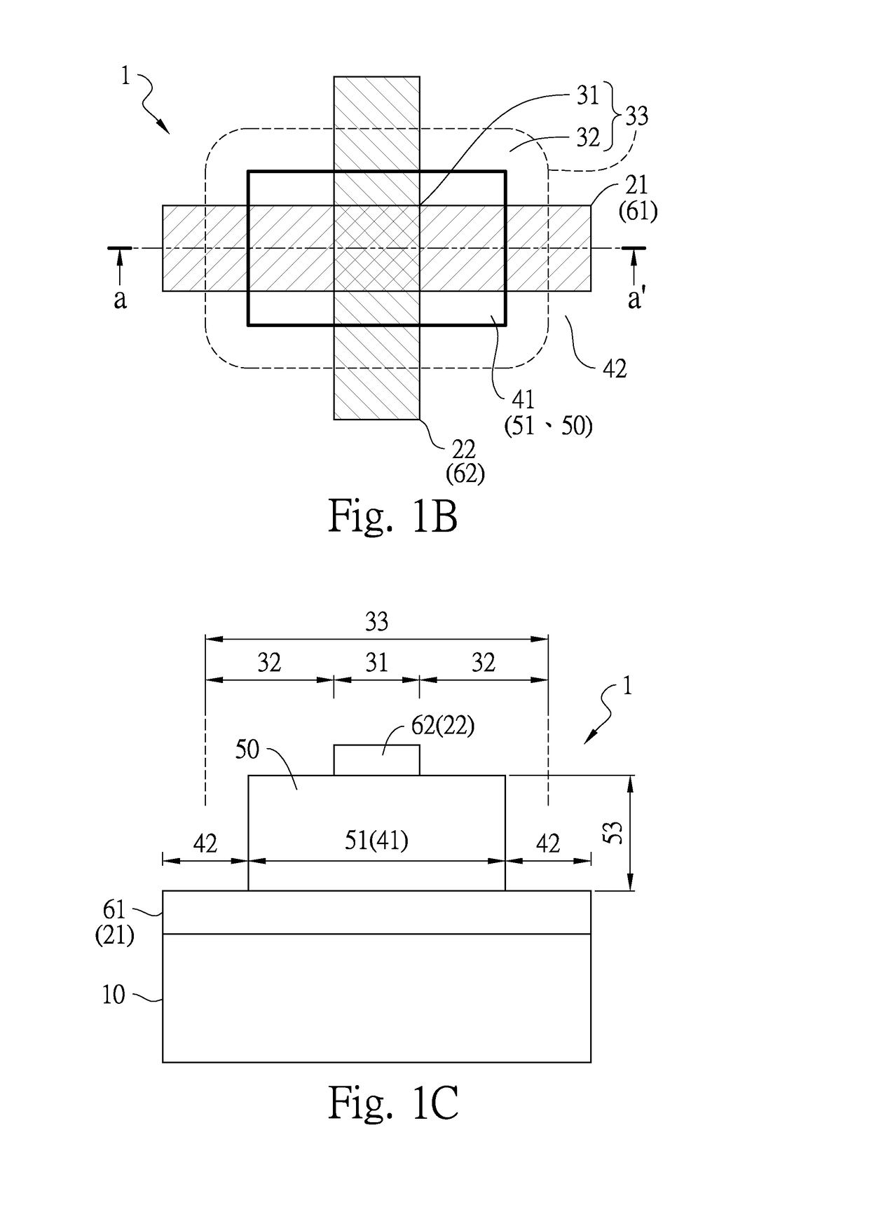
[0079]Please refer to FIGS. 1 and 1A (along the broken line a-a′ in FIG. 1) which show, respectively, the top view and the cross-sectional view of an embodiment of a layout method for compound semiconductor integrated circuits of the present invention. A compound semiconductor integrated circuit layout area 1 is defined on a top surface of a compound semiconductor substrate 10, wherein the compound semiconductor integrated circuit layout area 1 includes a first circuit layout area 21 and a second circuit layout area 22. A first metal layer 61 is formed within the first circuit layout area 21. The first circuit layout area 21 and the second circuit layout area 22 intersect at an intersection area 31. An adjacent crossover area 33 is defined to include the intersection area 31 and a peripheral adjacent area 32 of the intersection area 31. A first dielectric area 41 (the thick border frame area) is defined on the top surface of the compound semiconductor substrate 10, wherein the first...


PUM


Abstract

A layout method for compound semiconductor integrated circuits, comprising following steps of: forming a first metal layer within a first circuit layout area which intersects with a second circuit layout area at an intersection area on a compound semiconductor substrate; defining an adjacent crossover area including said intersection area and a peripheral adjacent area thereof; a first dielectric area located within said adjacent crossover area and intersected with at least part of said intersection area; forming a first dielectric block within said first dielectric area or forming said first dielectric block within said first dielectric area and a second dielectric block outside said first dielectric area, the thickness of said second dielectric block is no greater than and the thickness of at least part of said second dielectric block is smaller than the thickness of said first dielectric block; forming a second metal layer within said second circuit layout area.

Description

FIELD OF THE INVENTION[0001]The present invention relates to a layout method for compound semiconductor integrated circuits, especially to a layout method for compound semiconductor integrated circuits with enhanced moisture resistance ability for the compound semiconductor integrated circuits.BACKGROUND OF THE INVENTION[0002]In the compound semiconductor integrated circuits, when two metal layers having different potentials is required to cross-connect, the area of the cross-connection between two metal layers requires good isolation. Conventional technology forms an isolation layer made of polyimide to isolate the cross-connection of two metal layers having different potentials. Usually an isolation layer of polyimide is firstly formed on a bottom metal layer, and then forming a top metal layer on the polyimide isolation layer, wherein the bottom metal layer and the top metal layer are two metal layers having different potentials. However, the polyimide isolation layer is needed o...

Claims


Application Information

Patent Timeline
Patent Type & Authority Applications(United States)
IPC IPC(8): H01L23/522H01L23/00H01L21/762
CPCH01L23/5221H01L23/564H01L21/762H01L23/5223H01L27/0207H01L27/0823H01L29/0692H01L29/42304H01L29/66242H01L29/73H01L29/737H01L29/7371
Inventor TSAI, SHU-HSIAOSYU, RONG-HAOLIU, YI-LINGLIN, CHENG-KUO
Owner WIN SEMICON
Learn More