Overlay mask

a mask and overlay technology, applied in the field of integrated circuits, can solve the problems of improving the integrity of overlay marks between multiple pre-layers, compromising ic performance, etc., and achieve the effect of saving overlay measurement time and higher area utilization efficiency of overlay marks

Active Publication Date: 2017-04-27
UNITED MICROELECTRONICS CORP
View PDF13 Cites 4 Cited by
  • Summary
  • Abstract
  • Description
  • Claims
  • Application Information

AI Technical Summary

Benefits of technology

[0008]It is one of the primary objectives of the present invention to provide an overlay mask, so as to improve diversity in mark design, and to further avoid signal missing or overlay issues.
[0011]According above, the overlay mask of the present invention includes patterns defined on different layers through different exposure steps. Since the linear patterns defined by at least two layers are disposed together within the same pitch, the arrangement of the overlay mask may be more diverse, and the overlay measurement is more convenient so as to effectively save the overlay measurement time. Thus, the area utilization efficiency of the overlay mark is higher than the conventional overlay mark in the present invention.

Problems solved by technology

However, in ICs with multiple layers, displacement between non-adjacent layers may compromise IC performance.
Therefore, improving the integrity of overlay marks between multiple pre-layers is still an important issue in the field.

Method used


Image

  • Overlay mask
  • Overlay mask
  • Overlay mask

Examples


Embodiment Construction

[0021]To provide a better understanding of the present invention, preferred embodiments will be described in detail. The preferred embodiments of the present invention are illustrated in the accompanying drawings with numbered elements.

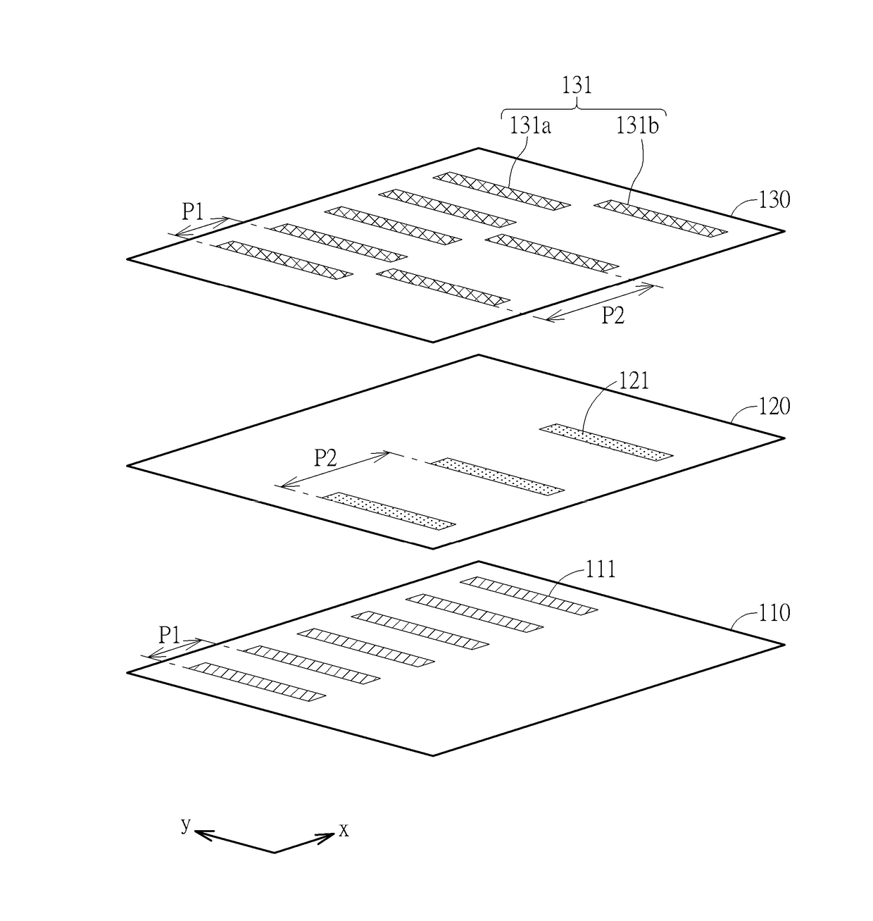
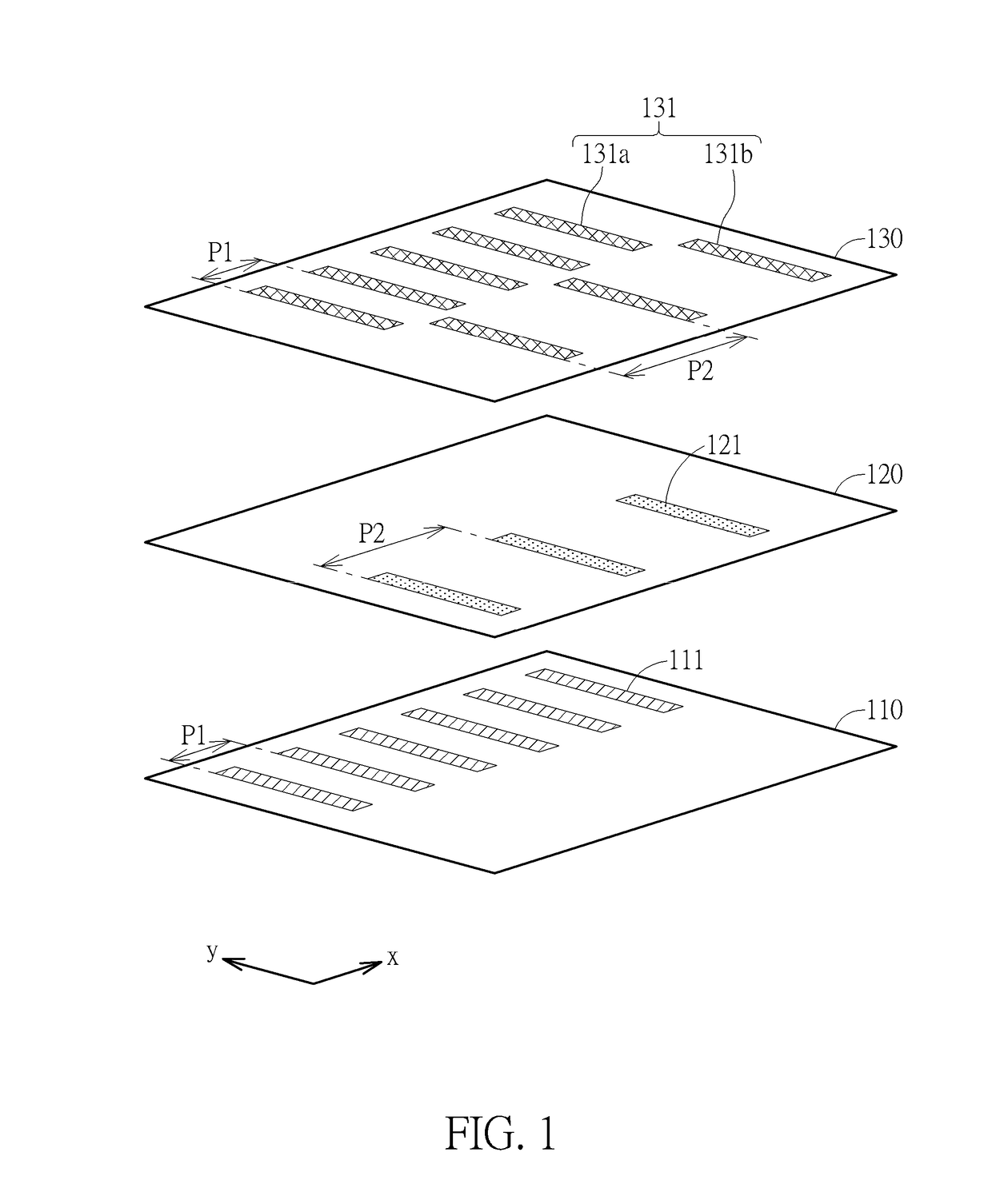
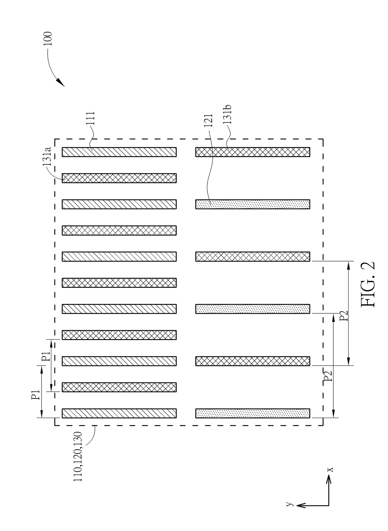
[0022]Referring to FIG. 1 to FIG. 3, which are schematic diagrams illustrating a method of forming an overlay mask according to the first preferred embodiment of the present invention, which may include sequentially forming a plurality of first patterns 111, second patterns 121 and third patterns 131 for example through three different exposure steps. In one embodiment, the first patterns 111, the second patterns 121 and the third patterns 131 may be respectively formed on three different layers 110, 120, 130, and relationships among the three different layers 110, 120, 130 are illustrated, for example being vertically and sequentially arranged, as shown in FIG. 1, but is not limited thereto. People skilled in the art shall easily realize that the fir...


PUM

PropertyMeasurementUnit
displacementaaaaaaaaaa
area utilization efficiencyaaaaaaaaaa
conductiveaaaaaaaaaa

Abstract

An overlay mask includes a plurality of first patterns, a plurality of second patterns and a plurality of third patterns. The first patterns are arranged within a first pitch. The second patterns are arranged within a second pitch. A first portion of the third patterns are arranged alternately with the first patterns, within the first pitch, and a second portion of the third patterns are arranged alternately with the second patterns, within the second pitch, and the first pitch is not equal to the second pitch.

Description

CROSS REFERENCE TO RELATED APPLICATIONS[0001]This application is a Divisional of application Ser. No. 14 / 920,859 filed Oct. 22, 2015, and included herein by reference.BACKGROUND OF THE INVENTION[0002]1. Field of the Invention[0003]The present invention relates to an integrated circuit (IC), and more particularly to an overlay mark used for alignment accuracy measurement in an IC.[0004]2. Description of the Prior Art[0005]As the linewidth of the IC process continuously gets narrower, the alignment accuracy between a lower layer and an upper layer becomes more and more important. Therefore, an overlay mark is generally formed on a wafer to check alignment accuracy.[0006]A conventional overlay mark typically includes x-directional linear patterns and y-directional linear patterns of a single pre-layer, and x-directional linear patterns and y-directional linear patterns of the current layer. Overlay errors have been measured only between two adjacent layers.[0007]However, in ICs with mu...

Claims


Application Information

Patent Timeline
Patent Type & Authority Applications(United States)
IPC IPC(8): G03F7/20
CPCG03F7/70633H01L21/02642H01L21/027H01L21/266H01L21/308H01L21/3081H01L21/3085H01L21/3086H01L21/3088H01L21/31144H01L21/32139
Inventor LIN, CHE-YILIOU, EN-CHIUANWANG, YI-JINGTSENG, CHIA-HSUN
Owner UNITED MICROELECTRONICS CORP
Why Eureka
Try Eureka