
Semiconductor device and semiconductor system

Active Publication Date: 2017-04-27
SK HYNIX INC
View PDF0 Cites 0 Cited by
  • Summary
  • Abstract
  • Description
  • Claims
  • Application Information

AI Technical Summary

Benefits of technology

The patent text describes embodiments of a semiconductor device and system that can write data by combining logic levels. The system can recover the original logic levels during a read operation, reducing interference between data bits and improving the quality of the data. This technology helps to minimize inter-symbol interference and inter-channel interference, resulting in more reliable and accurate data transmission.

Problems solved by technology

In this way, as the size of memory cells disposed in a semiconductor device and the width of lines through which data are transmitted decrease, interference between data bits increases.

Method used


Image

  • Semiconductor device and semiconductor system
  • Semiconductor device and semiconductor system
  • Semiconductor device and semiconductor system

Examples


Embodiment Construction

[0025]Hereinafter, a semiconductor device and a semiconductor system will be described below with reference to the accompanying drawings through various examples of embodiments.

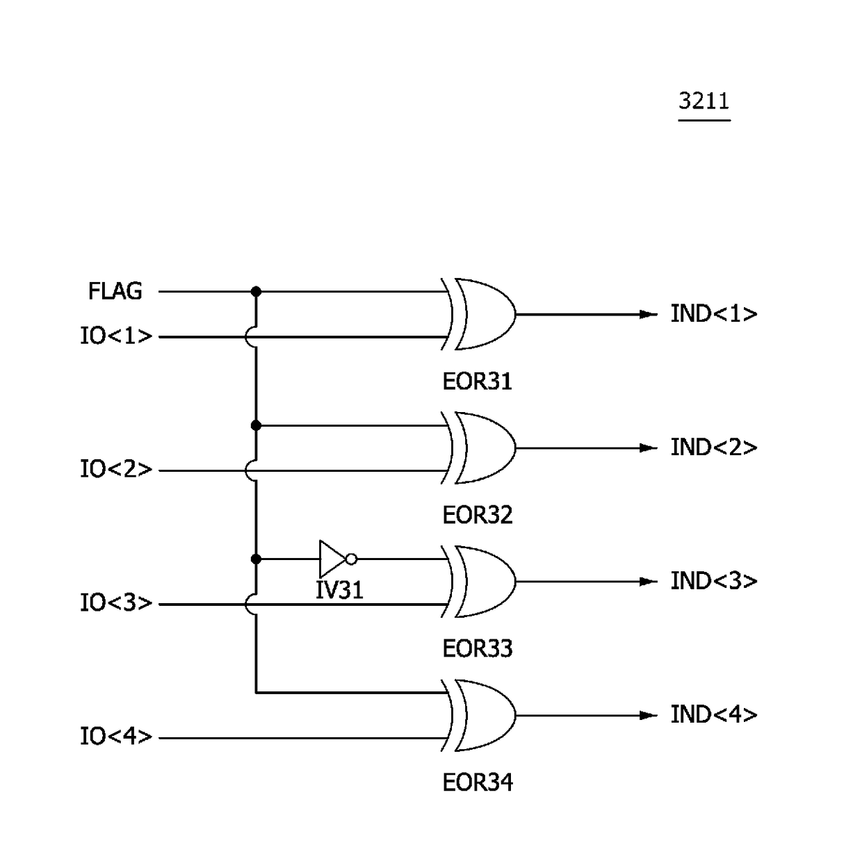
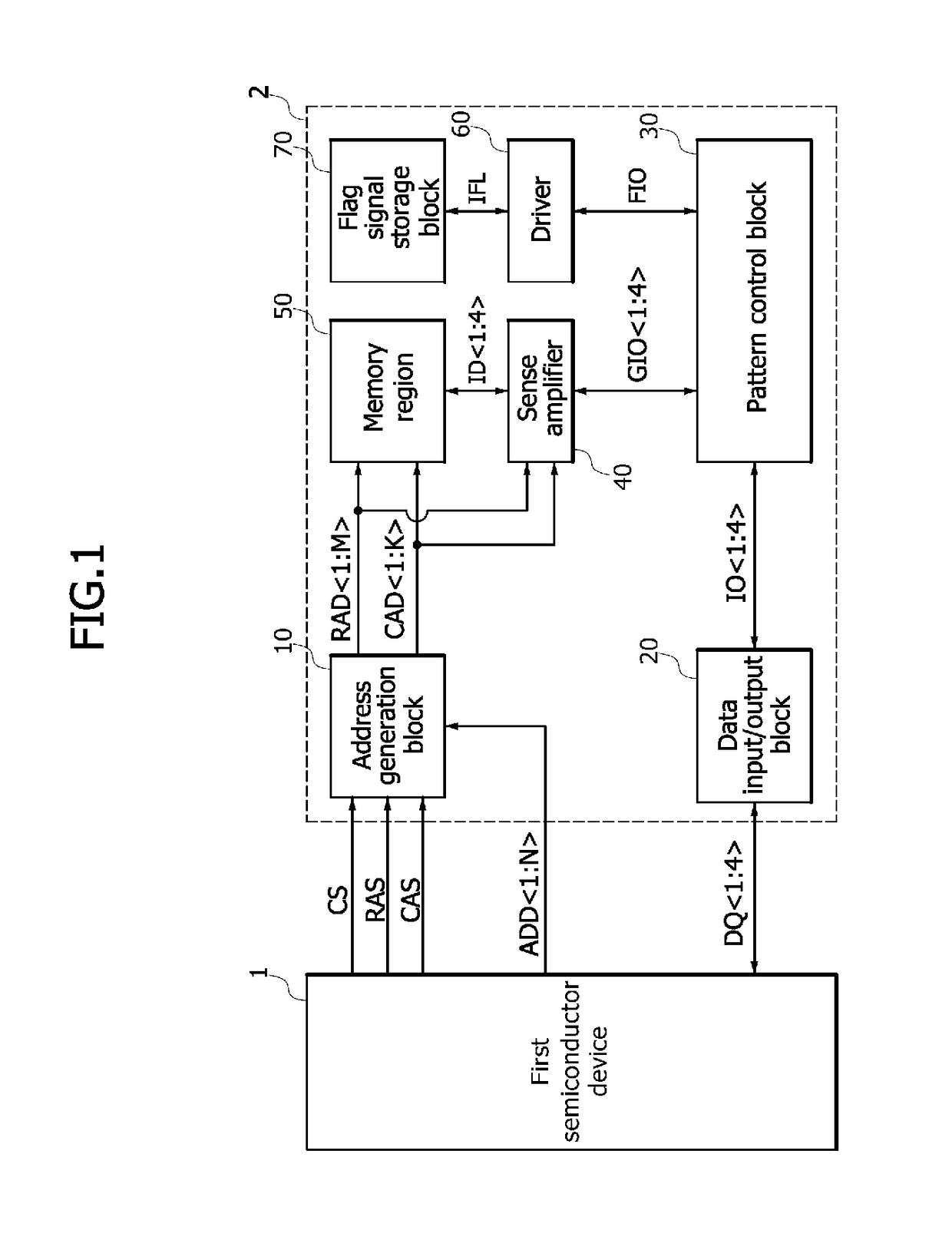
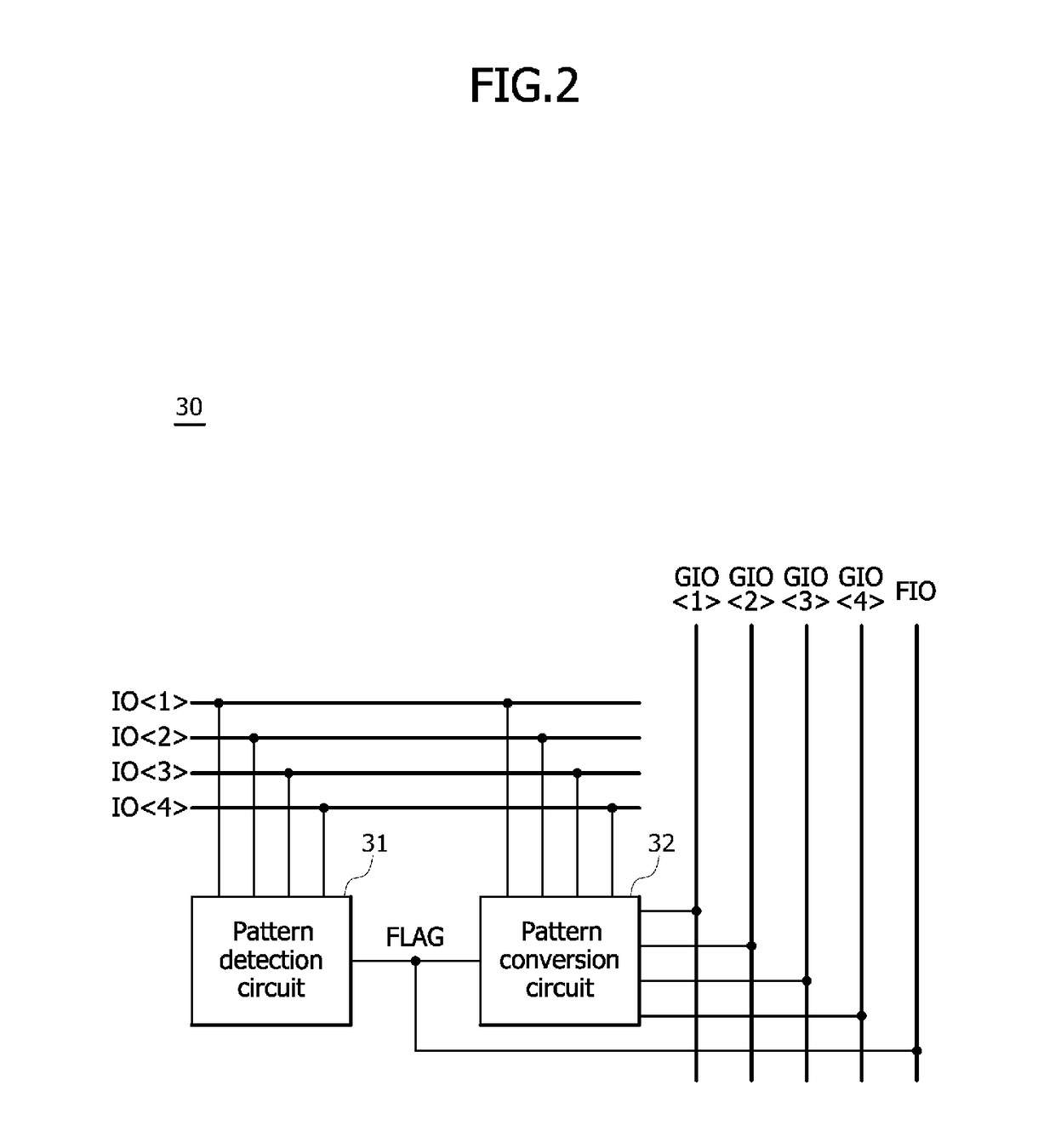
[0026]Referring to FIG. 1, a semiconductor system in accordance with an embodiment may include a first semiconductor device 1 and a second semiconductor device 2. The second semiconductor device 2 may include an address generation block 10, a data input / output block 20, a pattern control block 30, a sense amplifier 40, a memory region 50, a driver 60, and a flag signal storage block 70.

[0027]The first semiconductor device 1 may output commands CS, RAS and CAS, first to Nth addresses ADD, and first to fourth data DQ. The first semiconductor device 1 may receive first to fourth data DQ. The commands CS, RAS and CAS may be transmitted through lines through which at least ones of addresses, commands and data are transmitted. Also, the commands CS, RAS and CAS may be successively transmitted through one line. The ...


PUM


Abstract

A semiconductor system may include a first semiconductor device configured to output commands, addresses and data. The semiconductor system may include a second semiconductor device configured to convert a logic level combination of the data when only any one of bits of the data is a different logic level, and store the data in response to the commands and the addresses, in a write operation.

Description

CROSS-REFERENCE TO RELATED APPLICATION[0001]The present application claims priority under 35 U.S.C. §119(a) to Korean Patent Application No. 10-2015-0149657, filed on Oct. 27, 2015, in the Korean Intellectual Property Office, which is incorporated herein by reference in its entirety.BACKGROUND[0002]1. Technical Field[0003]Embodiments of the present disclosure generally relate to a semiconductor device and a semiconductor system, and, more particularly, to a semiconductor device and a semiconductor system which input and output data by converting a logic level combination thereof.[0004]2. Related Art[0005]In general, a semiconductor device includes a plurality of memory cells. The semiconductor device including the memory cells may perform a write operation and a read operation to store data in the memory cells and to output data stored in the memory cells to an exterior. The write operation or the read operation can be performed in accordance with control from a controller.[0006]As ...

Claims


Application Information

Patent Timeline
IPC IPC(8): G11C7/10G11C8/10G11C7/12G11C7/06
CPCG11C7/1063G11C7/06G11C7/10G11C7/1084G11C7/12G11C7/1057G11C8/10G11C7/1078G11C7/02G11C7/08G11C7/1006G11C29/1201G11C29/18G11C29/36G11C29/44G11C29/56008G11C29/56012G11C2029/1208G11C2029/4402
Inventor PARK, MIN SOOKIM, JIN SENA, MOON YUBCHOI, MIN JUNHAN, HYUN WOOK
Owner SK HYNIX INC
Features
  • Generate Ideas
  • Intellectual Property
  • Life Sciences
  • Materials
  • Tech Scout
  • Unparalleled Data Quality
  • Higher Quality Content
  • 60% Fewer Hallucinations
Learn More