Semiconductor device

a technology of semiconductor devices and semiconductors, applied in semiconductor devices, semiconductor/solid-state device details, electrical apparatus, etc., can solve the problems of difficult reduction, inability to reduce the area occupied by circuits, and inability to reduce parasitic resistan

Active Publication Date: 2017-05-04
UNISANTIS ELECTRONICS SINGAPORE PTE LTD
View PDF2 Cites 1 Cited by
  • Summary
  • Abstract
  • Description
  • Claims
  • Application Information

AI Technical Summary

Benefits of technology

[0026]The semiconductor device may include a second insulating film between the first gate insulating film and the semiconductor-metal compound layer. By covering the semiconductor-metal compound with the second insulating film, it is possible to prevent the first gate insulating film from being contaminated with a metal.

Problems solved by technology

With such a miniaturization of MOS transistors, there may be a problem in that it becomes difficult to reduce a leakage current and the area occupied by circuits is not easily decreased from the viewpoint of ensuring a required amount of current.
However, only the diffusion layer is disposed between a lower portion of the pillar-shaped semiconductor layer and the outside of the insulating film that is formed, as the sidewall, on the side wall of the gate electrode, and thus a reduction in the parasitic resistance has not been realized.

Method used


Image

  • Semiconductor device
  • Semiconductor device

Examples


Embodiment Construction

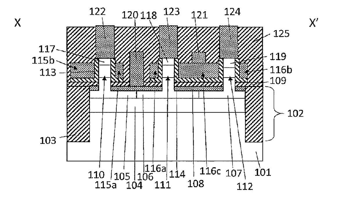
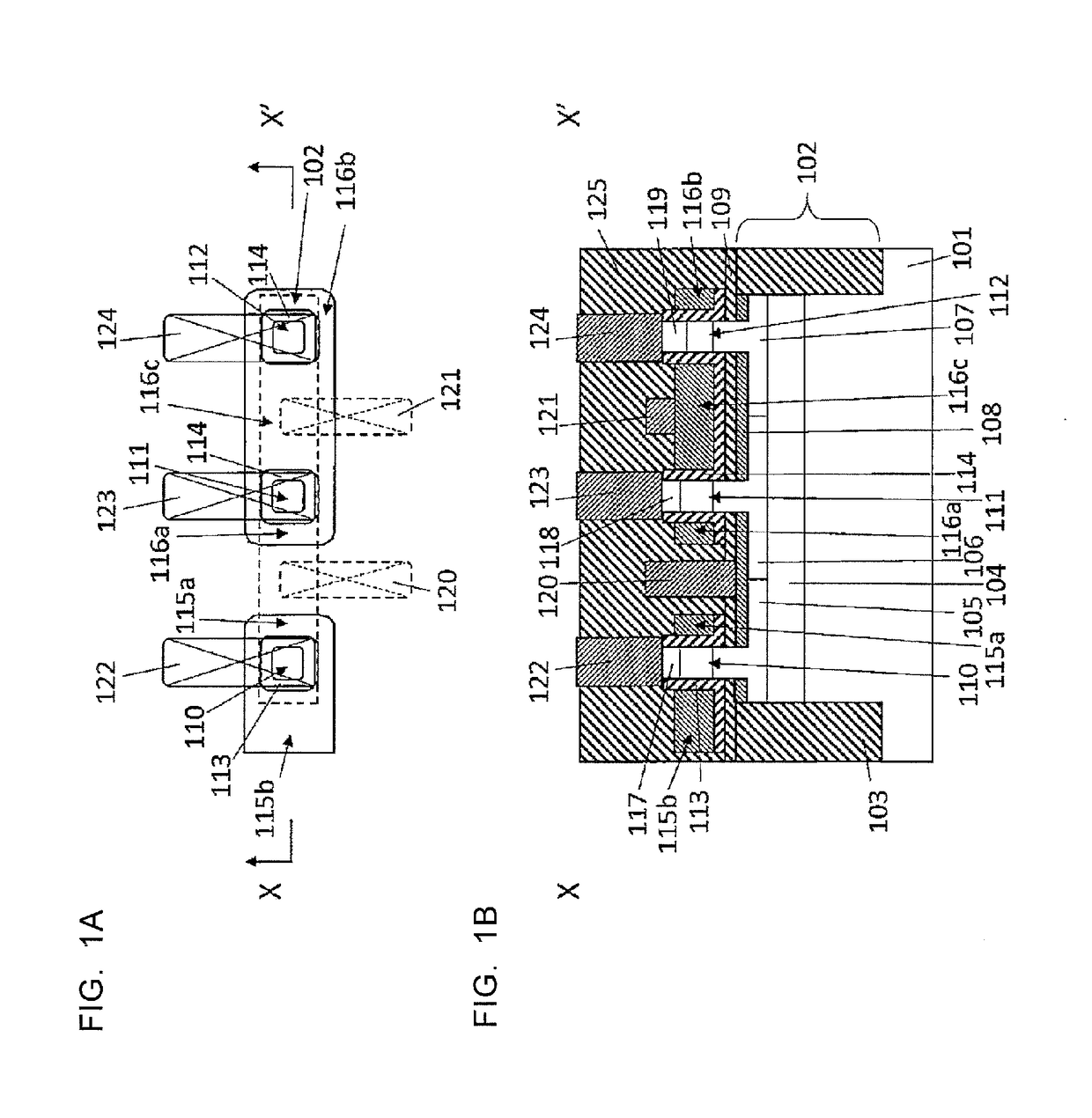
[0029]A semiconductor device according to an embodiment of the present invention will now be described with reference to FIGS. 1A and 1B. Semiconductor layers of the present embodiment are preferably silicon layers. The semiconductor layers may be made of a group IV semiconductor such as Ge or C. Alternatively, the semiconductor layers may be made of a group III-V compound semiconductor.

[0030]A semiconductor device includes a planar interconnection layer 102 formed on a substrate 101 and made of a semiconductor, a first pillar-shaped semiconductor layer 112 formed on the interconnection layer 102, a semiconductor-metal compound layer 108 formed so as to cover the entire upper surface of the interconnection layer 102 except for a bottom portion of the first pillar-shaped semiconductor layer 112, a first gate insulating film 114 surrounding the first pillar-shaped semiconductor layer 112, a first gate electrode 116b surrounding the first gate insulating film 114, and a first gate line...


PUM


Abstract

A semiconductor device includes a planar interconnection layer formed on a substrate and made of a semiconductor, a first pillar-shaped semiconductor layer formed on the interconnection layer, a semiconductor-metal compound layer formed so as to cover the entire upper surface of the interconnection layer except for a bottom portion of the first pillar-shaped semiconductor layer, a first gate insulating film surrounding the first pillar-shaped semiconductor layer, a first gate electrode surrounding the first gate insulating film, and a first gate line connected to the first gate electrode.

Description

CROSS-REFERENCE TO RELATED APPLICATION[0001]The present application is a continuation application of PCT / JP2015 / 080952, filed Nov. 2, 2015, the entire contents of which are incorporated herein by reference.BACKGROUND OF THE INVENTION[0002]1. Field of the Invention[0003]The present invention relates to a semiconductor device.[0004]2. Description of the Related Art[0005]The degree of integration of semiconductor integrated circuits, in particular, integrated circuits that use metal-oxide-semiconductor (MOS) transistors, has been increasing. With the increase in the degree of integration, MOS transistors used in the integrated circuits have been miniaturized to the nanometer scale. With such a miniaturization of MOS transistors, there may be a problem in that it becomes difficult to reduce a leakage current and the area occupied by circuits is not easily decreased from the viewpoint of ensuring a required amount of current. In order to address this problem, a surrounding gate transisto...

Claims


Application Information

Patent Timeline
Patent Type & Authority Applications(United States)
IPC IPC(8): H01L23/522H01L23/532H01L27/11H01L29/423H01L29/786
CPCH01L23/5228H01L29/42392H01L29/78642H01L23/53271H01L27/1104H01L27/1116H01L23/5226H01L29/78618H10B10/12H10B10/18
Inventor MASUOKA, FUJIONAKAMURA, HIROKIHARADA, NOZOMU
Owner UNISANTIS ELECTRONICS SINGAPORE PTE LTD
Why Eureka
Try Eureka