Storage device and storage unit

a storage device and storage unit technology, applied in semiconductor devices, digital storage, instruments, etc., can solve the problems of difficult to retain the intermediate resistance value for a long time, the resistance variation (random telegraph noise) is likely to occur in every reading, and the oxygen defect formed in writing tends to be repeatedly generated and disappeared, so as to improve the thermal and chemical stability of the conductive path, and reduce the effect of conductive path deteriorati

Inactive Publication Date: 2017-05-04
SONY CORP
View PDF4 Cites 1 Cited by
  • Summary
  • Abstract
  • Description
  • Claims
  • Application Information

AI Technical Summary

Benefits of technology

[0010]Therefore, it is desirable to provide a storage device and a storage unit that are capable of improving retention performance of an intermediate resistance value in writing at a low current. Moreover, it is desirable to provide a storage device and a storage unit that are capable of reducing random telegraph noise.
[0016]In the storage device of the one embodiment of the present technology or the storage unit of the one embodiment of the present technology, as constituent materials of the resistance change layer, boron (B) and oxygen (O) are used to form a bond between O and B, thereby improving thermal and chemical stability of the conductive path.
[0017]In the storage device of the other embodiment of the present technology or the storage unit of the other embodiment of the present technology, the chalcogen element and the Group 4, 5, and 6 transition metal elements in the periodic table are used for the ion source layer, and as with the ion source layer, the Group 4, 5, and 6 transition metal elements in the periodic table are used for the resistance change layer. Therefore, charge deviation around an oxygen defect formed in writing is stabilized.
[0018]According to the storage device of the one embodiment of the present technology or the storage unit of the one embodiment of the present technology, boron (B) and oxygen (O) are used as constituent materials of the resistance change layer. Accordingly, a bond between B and O with large binding energy is formed, and thermal and chemical stability of the conductive path is improved. Therefore, retention performance of an intermediate resistance value in writing at a low current of the resistance change layer is allowed to be improved.
[0019]According to the storage device of the other embodiment of the present technology or the storage unit of the other embodiment of the present technology, the chalcogen element with a large relative dielectric constant is used for the ion source layer, and the ion source layer and the resistance change layer each include a metal element of a same kind (Group 4, 5, and 6 transition metal elements in the periodic table). Therefore, charge deviation around an oxygen defect formed in writing is allowed to be stabilized, and random telegraph noise is allowed to be reduced.

Problems solved by technology

However, since the above-described storage device does not have sufficient thermal and chemical stability, it is difficult to retain the intermediate resistance value for a long time.
Moreover, an oxygen defect formed in writing tends to be repeatedly generated and disappear, and as a result, there is an issue that resistance variation (random telegraph noise) is likely to occur in every reading.
This is because charge deviation around the oxygen defect is difficult to stably exist.

Method used


Image

  • Storage device and storage unit
  • Storage device and storage unit
  • Storage device and storage unit

Examples


first embodiment (

1. First Embodiment (An example in which a resistance change layer includes boron (B) and oxygen (O))

1-1. Storage Device

1-2. Storage Unit

[0030]2. Modification Example 1 (An example in which a resistance change layer has a laminate configuration)

second embodiment (

3. Second Embodiment (An example in which an ion source layer and a resistance change layer each include a transition metal element)

4. Modification Example 2 (An example in which a resistance change layer has a laminate configuration)

5. Examples

first embodiment

1 FIRST EMBODIMENT

(1-1. Storage Device)

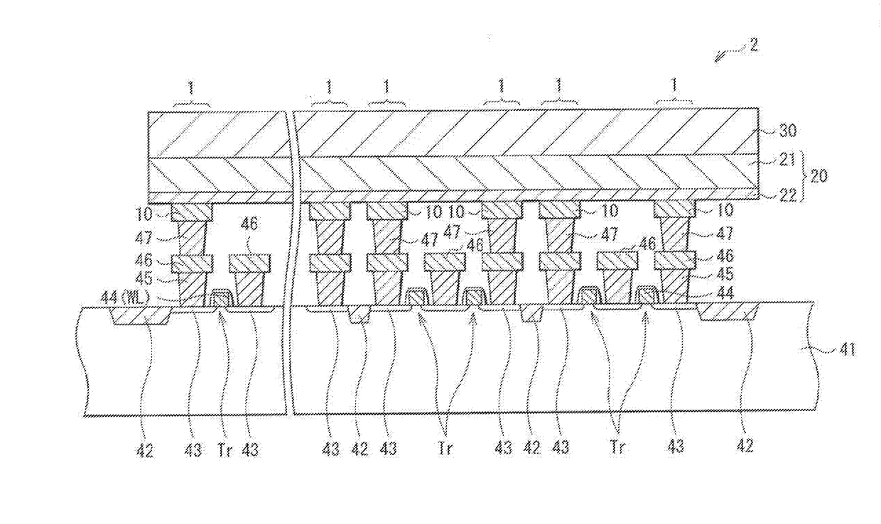
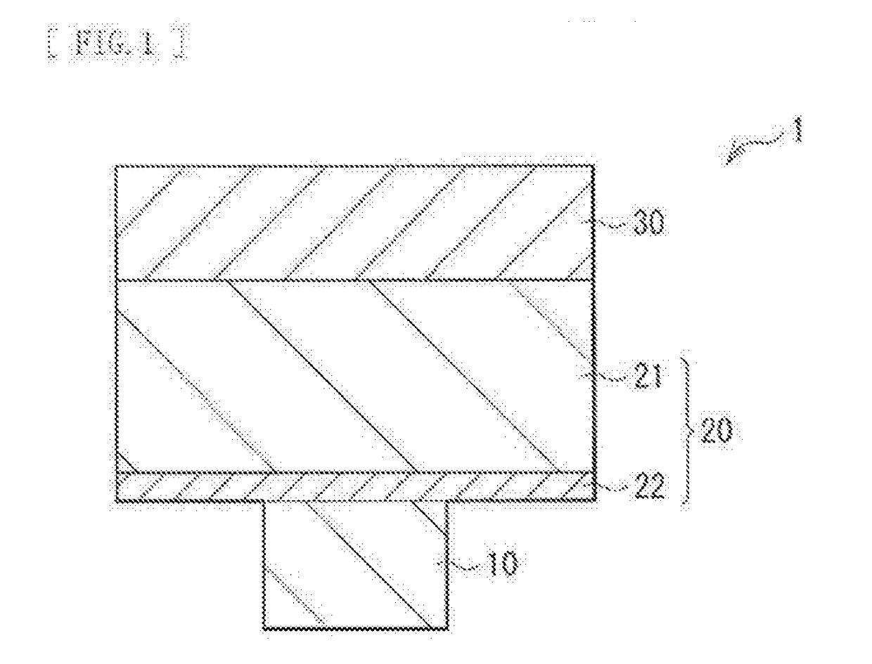
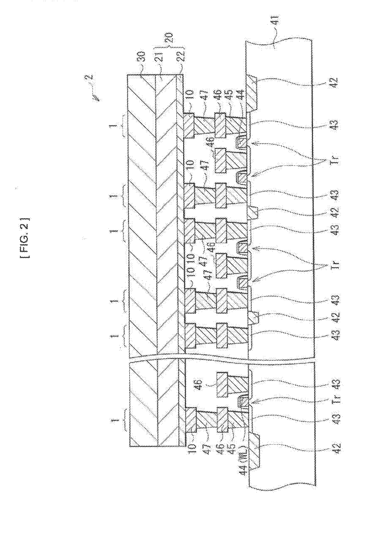
[0031]FIG. 1 illustrates a sectional configuration of a storage device 1 according to a first embodiment of the present disclosure. This storage device 1 includes a lower electrode 10 (a first electrode), a storage layer 20 including an ion source layer 21, and an upper electrode 30 (a second electrode) in this order.

[0032]For example, as will be described later (FIG. 2), the lower electrode 10 is provided on a substrate 41 that may be made of silicon and in which a CMOS (Complementary Metal Oxide Semiconductor) circuit may be formed, and may serve as a connection section with the CMOS circuit. This lower electrode 10 may be made of a wiring material for use in a semiconductor process, for example, tungsten (W), tungsten nitride (WN), copper (Cu), aluminum (Al), molybdenum (Mo), tantalum (Ta), silicide, or the like. In a case where the lower electrode 10 is made of a material, such as Cu, that may cause ion conduction by an electrical field, a ...


PUM


Abstract

There are provided a storage device and a storage unit capable of improving retention performance of an intermediate resistance value in writing at a low current, and a storage device and a storage unit capable of reducing random telegraph noise. A storage device of one embodiment of the present technology includes a first electrode, a storage layer, and a second electrode in this order, and the storage layer includes: an ion source layer including one or more kinds of chalcogen elements selected from tellurium (Te), sulfur (S), and selenium (Se), and one or more kinds of transition metal elements selected from Group 4 elements, Group 5 elements, and Group 6 elements of the periodic table; and a resistance change layer including boron (B) and oxygen (O). A storage device of another embodiment of the present technology includes the above-described ion source layer and a resistance change layer including one or more kinds of transaction metal elements selected from Group 4 elements, Group 5 elements, and Group 6 elements of the periodic table, and oxygen (O).

Description

CROSS REFERENCE TO RELATED APPLICATIONS[0001]The present application is a continuation application of U.S. patent application Ser. No. 14 / 647,793 filed May 27, 2015, which is a National Stage of PCT / JP2013 / 079983 filed Nov. 6, 2013, and claims the benefit of priority from Japanese Patent Application No. JP 2012-264168 and JP 2013-141685 respectively filed in the Japanese Patent Office on Dec. 3, 2012 and Jul. 5, 2013, the entire content of which is hereby incorporated by reference.TECHNICAL FIELD[0002]The present disclosure relates to a storage device and a storage unit that hold information by change in electrical characteristics of a storage layer including an ion source layer.BACKGROUND ART[0003]NOR or NAND flash memories have been typically used as semiconductor nonvolatile memories for data storage. These semiconductor nonvolatile memories have achieved an increase in capacity by miniaturizing memory devices and drive transistors; however, since a high voltage is necessary for ...

Claims


Application Information

Patent Timeline
Patent Type & Authority Applications(United States)
IPC IPC(8): H01L45/00G11C13/00H01L27/24
CPCH01L45/085H01L45/1233H01L45/147H01L45/144H01L45/143H01L45/142H01L27/2463G11C13/0007G11C13/004G11C2213/31G11C2213/56G11C2213/35G11C13/0069H10B63/82H10B63/30H10N70/245H10N70/24H10N70/826H10N70/883G11C13/0009G11C13/0004H10B63/80H10N70/8822H10N70/8825H10N70/8828H10N70/8836
Inventor OHBA, KAZUHIROSEI, HIROAKI
Owner SONY CORP
Why Eureka
Try Eureka