Latch circuit and double data rate decoding device based on the same

a decoding device and latch circuit technology, applied in the field of latch circuit and double data rate decoding device, can solve the problem that the size of the cmos image sensor needs to be sufficiently large to accommodate the plurality of address lines

Active Publication Date: 2017-05-11
SK HYNIX INC
View PDF5 Cites 3 Cited by
  • Summary
  • Abstract
  • Description
  • Claims
  • Application Information

AI Technical Summary

Benefits of technology

[0033]When the output of the next latch stage is changed to a high level, the feedback input unit may receive a negative output of the next latch stage and change an output of a current latch stage to a low level according to the shifting clock.

Problems solved by technology

The described conventional address decoding scheme may select a desired line using an input address, but may be disadvantageous in that the size of the CMOS image sensor needs to be sufficiently large to accommodate the plurality of address lines.

Method used


Image

  • Latch circuit and double data rate decoding device based on the same
  • Latch circuit and double data rate decoding device based on the same
  • Latch circuit and double data rate decoding device based on the same

Examples


Embodiment Construction

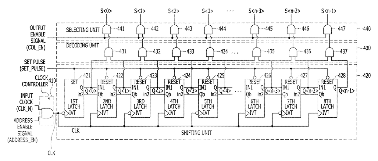
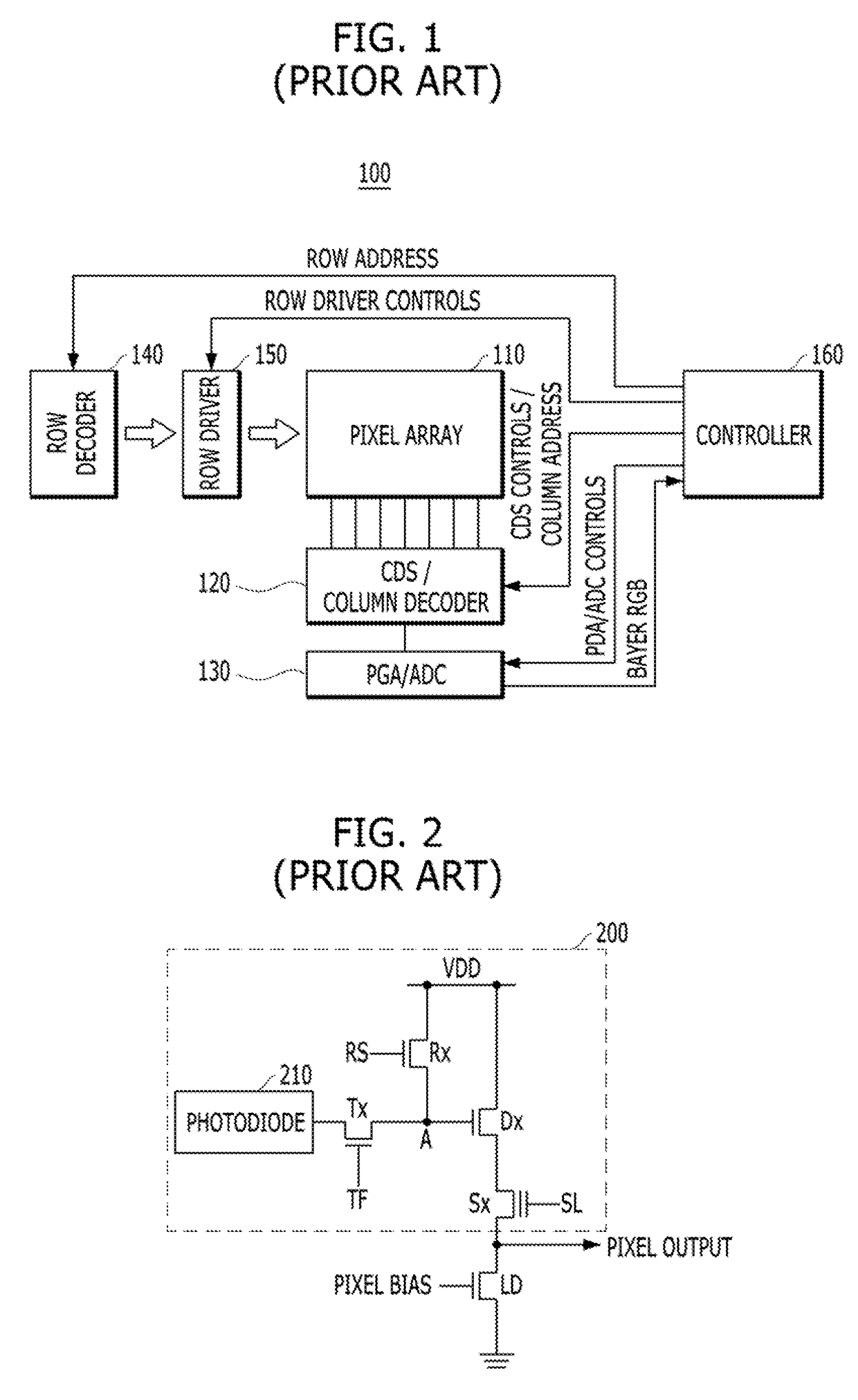
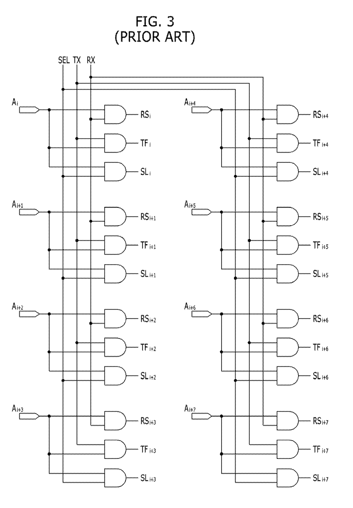
[0045]Various embodiments of the present invention will be described below in more detail with reference to the accompanying drawings. The present invention may, however, be embodied in different forms and should not be construed as being limited to the embodiments set forth herein. Rather, these embodiments are provided so that this disclosure will be thorough and complete. Throughout the disclosure, like reference numerals refer to like parts throughout the various figures and embodiments of the present invention.

[0046]In this disclosure, when one part is referred to as being ‘connected’ to another part, it should be understood that the former can be ‘directly connected’ to the latter, or ‘electrically connected’ to the latter via an intervening part. Furthermore, the terms ‘comprises’, ‘includes’ or ‘has’ and the like when used herein should be understood as being inclusive terms allowing the presence of other elements in addition to the elements expressly stated. Moreover, singu...


PUM


Abstract

Disclosed are a latch circuit receiving a negative output of a next latch stage circuit as a feedback input, a double data rate (DDR) ring counter based on the latch circuit to perform DDR counting of pulse periods and reduce the number of toggles, a hybrid counting device counting lower-bit portion by using the latch-based DDR ring counter and upper-bit portion by using a binary counter, and an analog-to-digital converting device and a CMOS image sensor employing the hybrid counting device. A double data rate ring counter may include a plurality of latches coupled in a form of a ring. The plurality of latches may include positive-edge-triggered latches and negative-edge-triggered latches arranged alternately. A current latch stage receives an output of a preceding latch stage to shift to a next latch stage according to a counter clock, receives an output of the next latch stage to check a data shift to the next latch stage, and falls to a low level if the data shift is checked.

Description

CROSS-REFERENCE TO RELATED APPLICATIONS[0001]The present application claims priority of Korean Patent Application No. 10-2015-0156608, filed on Nov. 9, 2015, which is incorporated herein by reference in its entirety.BACKGROUND[0002]1. Field[0003]Various embodiments of the present invention relate generally to a decoding device suitable for shifting addresses in a device such as a CMOS image sensor and, more particularly, to a latch circuit and a double data rate decoding device implemented based on the latch circuit.[0004]2. Description of the Related Art[0005]A CMOS image sensor (CIS) captures an image using a property of semiconductor material that it responds to an incident light. The CMOS image sensor may include an array of multiple pixels, each of which may have an image sensing element, such as a photodiode, and a plurality of transistors. The CMOS image sensor may generate an electric image signal corresponding to the incident light.[0006]FIG. 1 is a block diagram of a typic...

Claims


Application Information

Patent Timeline
Patent Type & Authority Applications(United States)
IPC IPC(8): G11C7/10G11C8/18H03K3/037
CPCG11C7/10H03K3/037G11C7/1087G11C7/106G11C8/18H04N25/76H04N25/77G11C19/28H03K3/356026
Inventor HWANG, WON-SEOK
Owner SK HYNIX INC
Why Eureka
Try Eureka